COA Tutorial (Gate Wallah) ▶️
Topics
Section titled “Topics”- [[#CA vs CO]]
- [[#Floating Point Representation]]
- [[#IEEE-754 Floating Point Representation (Standard Representation)]]
- [[#Single Precision Representation]]
- [[#Implicit Normalized vs Explicit Normalized (Optional⭐)]]
- [[#Denormalized (Subnormal) Number? (Optional⭐)]]
- [[#Implicit Normalized ⭐]]
- [[#Denormalized]]
- [[#Components of Computer]]
- [[#System Buses]]
- [[#CPU Registers]]
- [[#Micro Operations]]
- [[#Instructions]]
- Questions 1-4
- [[#Effective Address]]
- [[#Instruction Cycle]]
- [[#Two types of Instruction]]
- [[#Addressing Mode ⭐]]
- [[#Intra-segment vs Inter Segment (Optional ⭐)]]
- [[#Components]]
- [[#Arithmetic Logical Unit (ALU)]]
- [[#Control Unit (CU)]]
- [[#Hardwired Control Unit]]
- [[#Microprogrammed CU]]
- [[#Microinstruction & Control Word]]
- [[#Control Memory]]
- [[#Control Word Sequencing]]
- [[#Types of Microprogrammed CU]]
- [[#RISC vs CISC]]
- [[#Byte Ordering]]
- [[#I/O Devices]]
- [[#Need of Interface]]
- [[#IO vs Memory Buses]]
- [[#Memory Mapped IO vs IO Mapped IO]]
- [[#Asynchronous Serial Transfer]]
- [[#Modes of Transfer]]
- [[#1. Programmed I/O (PIO / Program-Controlled I/O)]]
- [[#2. Interrupt-Driven I/O]]
- [[#3. Direct Memory Access (DMA)]]
- [[#CPU Blocked in Different Modes (due to DMA)]]
- [[#Advantage / Disadvantage of Different Mode of Transfer (Optional ⭐)]]
- [[#Hierarchy of Memory]]
- [[#Memory Representation]]
- [[#Byte vs Word Addressable Memory]]
- [[#Main Memory]]
- [[#Types of RAM]]
- [[#Table for Multiplication & Addition]]
- [[#Multiple Chips in Single System]]
- [[#Vertical Arrangement]]
- [[#Horizontal Arrangement]]
- [[#Hybrid Arrangement]]
- [[#DRAM Refresh]]
- [[#Associative Memory]]
- [[#Locality of Reference]]
- [[#Cache Memory]]
- [[#Cache Access Types]]
- [[#Average Memory Access Time (AMAT)]]
- [[#Cache Write Policies]]
- [[#Write Through (No Write Allocate)]]
- [[#Write Back (Write Allocate)]]
- [[#Cache Mapping]]
- [[#Direct Mapping ⭐⭐]]
- [[#Checking Hit/Miss in Direct Mapping]]
- [[#Set Associative Mapping]]
- [[#Checking Hit/Miss in Set Associative Mapping]]
- [[#Fully Associative Mapping]]
- [[#Checking hit/miss in Fully Associative Mapping]]
- [[#Comparisons of Different Mapping Techniques]]
- [[#Transition From Direct to Fully Associative Mapping]]
- [[#Direct Mapping ⭐⭐]]
- [[#Cache Block Replacement]]
- [[#Cache Miss Penalty]]
- [[#Types of Cache Miss]]
- [[#Multilevel Cache]]
- [[#Cache Inclusion Policy]]
- [[#Dual Cache]]
- [[#Magnetic Disk]]
- [[#Sector Capacity]]
- [[#Disk Access Time]]
- [[#Disk Transfer Rate]]
- [[#DMA with Disk]]
- [[#Multiple Sectors Access Time]]
- [[#Cylinder]]
- [[#Disk Addressing in a Cylinder]]
- [[#Pipelining]]
- [[#Pipeline Cycle Time]]
- [[#Non-Pipelined Execution]]
- [[#Pipelined Execution]]
- [[#Special Cases]]
- [[#Synchronous Pipeline]]
- [[#Latency & Throughput]]
- [[#Stall in Pipelining ⭐]]
- [[#Instruction Pipeline (with Branch Stall)]]
- [[#Pipeline Hazard]]
- [[#Data Hazard Classification]]
- [[#Pipeline Efficiency]]
- [[#CPI (Cycles Per Instruction)]]
CA vs CO
Section titled “CA vs CO”Architecture (CA) -> Conceptual design & fundamental operational structure
- CPU Design, Instructions, Addressing Modes, Data Format
Organisation (CO -> Deals with physical devices and their instructions with a perspective of improving the performance
- I/O Organisation, Memory Organisation, Performance
| Computer Architecture | Computer Organization |
|---|---|
| CPU Design | I/O Organisation |
| Instructions | Memory Organisation |
| Addressing modes | Peformance |
| Data format |
- COA = CA(Design) + CO(Implementation) ⭐
Floating Point Representation
Section titled “Floating Point Representation”GATE Important & Smallest Topic -> Floating Point Representation
The number is represented in format:
Sign Exponent Manitissa┌────────┬─────────┬────────┐│ S │ E │ M │└────────┴─────────┴────────┘- Sign
0 +ve ⬈S ⬊ 1 -ve- Exponent it is stored in biased form
Original Exponent: eBiased Exponent : E
Biased E = e + biasoriginal e = E - bias- Mantissa is signed normalized (implicit/explicit) fraction number exponent
Implicit:
Original 1.M -> 1.xxxxxMantissa Stored M = xxxxx
Explicit is not important
IEEE-754 Floating Point Representation (Standard Representation)
Single Precision (Float in C)
<--------- 32 bits --------->┌────────┬─────────┬─────────┐│  1 bit │ 8 bits  │ 23 bits |└────────┴─────────┴─────────┘   S         E          M
bias = 127Value range (Exponent) = 1 to 254 ⭐
Double Precision (Double in C)
<--------- 64 bits --------->┌────────┬─────────┬─────────┐│  1 bit │ 11 bits │ 52 bits |└────────┴─────────┴─────────┘   S         E          M
bias = 1023Value range (Exponent) = 1 to 2046 ⭐
Biasing in Floating-point representation
If the number is unsigned:
- 8-bit: to => to
- 11-bit: to => to
For signed numbers / two’s complement (one bit for sign):
- 8-bit signed: to => to
- 11-bit signed: to => to
How bias works in floating-point representation:
- 8-bit exponent: possible values : to => to
- Bias = 127, => to => to
- 11-bit exponent: possible values to => to
- Bias = 1023, => to => to
Memory tip: Bias just shifts the exponent range so it can represent negative and positive powers of 2.
s
Single Precision Representation
Special Numbers
E = all 0'sorE = all 1's| S | E | M | 0.M /1.M | Number | Example for Single Precision |
|---|---|---|---|---|---|
| 0 | 00000000 | 000…0 | 1.M | +0 | |
| 1 | 00000000 | 000…0 | 1.M | -0 | |
| 0 | 11111111 | 000…0 | 1.M | +∞ | |
| 1 | 11111111 | 000…0 | 1.M | -∞ | |
| 0/1 | 11111111 | M ≠ 0…0 | 1.M | Not a Number (NaN) | → NaN |
| 0/1 | 00000000 | M ≠ 0…0 | 0.M | Denormalized | |
| 0/1 | 0…0 < E < 1…1 | x…x | 1.M | Normalized ⭐ |
- Bias = 127 (single precision)
- Exponent = all 1s
- M all 0s → Infinity
- M ≠ 0…0 → NaN
- Exponent = all 0s (use 0.M)
- M all 0s → Zero
- M ≠ 0…0 → Denormalized
- 0 < Exponent < all 1s (use 1.M)
- Any M → Normalized
Summary ⭐
| S | E | 0.M /1.M | M | Number |
|---|---|---|---|---|
| 0/1 | all 0’s | 1.M | all 0’s | +0 / -0 |
| 0/1 | all 1’s | 1.M | all 0’s | +∞ / -∞ |
| 0/1 | all 0’s | 0.M | M ≠ all 0’s | Denormalized |
| 0/1 | all 1’s | 1.M | M ≠ all 0’s | Not a Number (NaN) |
| 0/1 | Not all 0’s | 1.M | any | Implicit Normalized |
- Normal Case: Numbers are stored as implicitly normalized (leading 1 is hidden).
- Very Small Numbers: Stored as denormalized (leading 0, reduced precision).
- Very Large Numbers: Cannot be stored → treated as ∞ (overflow).
Implicit Normalized vs Explicit Normalized (Optional⭐)
| Aspect | Implicit Normalized ⭐ | Explicit (Non-Implicit) Normalized |
|---|---|---|
| Leading Bit | The leading 1 of the mantissa is not stored — it is assumed automatically. | The leading 1 of the mantissa is stored explicitly in memory. |
| Purpose | To save 1 bit of storage and still represent all normalized numbers. | To store the full mantissa explicitly (used in older or simpler systems). |
| Normalization Rule | Number is stored as 1.M × 2^(E − bias). | Number is stored as b.M × 2^(E − bias), where b (the leading bit) is stored in memory. |
| Efficiency | More efficient — one extra bit of precision gained. | Less efficient — one bit wasted storing the leading 1. |
| Example (Single Precision) | Mantissa bits in memory: M → actual value = 1.M. | Mantissa bits in memory: 1.M → actual value = 1.M. |
| Used In | IEEE-754 Floating Point (Single & Double Precision). | Non-IEEE or older custom floating-point formats. |
In short:
- Implicit normalized_ → hidden (assumed) leading 1.
- Explicit (non-implicit) normalized_ → leading 1 is stored in memory.
Denormalized (Subnormal) Number? (Optional⭐)
A denormalized (also called subnormal) number is a very small non-zero number that cannot be represented in the normalized (implicit) format — because the exponent would have to go below its minimum value.
Why It Exists
- In normalized form, exponent starts from
Emin = 1(not 0). - But what if you need to represent numbers smaller than
2^(-126)(for single precision)? - Denormalized numbers allow that — by removing the implicit 1 and fixing the exponent to its smallest possible value.
- This creates a smooth, gradual transition from the smallest normalized number down to zero.
How It Works
| Type | Exponent bits | Hidden bit | Formula | Range |
|---|---|---|---|---|
| Normalized | E ≠ 0, E ≠ all 1s | 1 (implicit) | (-1)^S × (1.M) × 2^(E−Bias) | ≈ 2^(−126) to ≈ 2^(+127) |
| Denormalized | E = 0 | 0 (no implicit 1) | (-1)^S × (0.M) × 2^(1−Bias) | ≈ 0 to ≈ 2^(−126) |
Example (Single Precision)
| Type | Binary Representation | Decimal Approx |
|---|---|---|
| Smallest Normalized | 1.000...0 × 2^(-126) | ≈ 1.175×10⁻³⁸ |
| Largest Denormalized | 0.111...1 × 2^(-126) | ≈ 1.175×10⁻³⁸ (just below normalized min) |
| Smallest Denormalized | 0.000...1 × 2^(-126) | ≈ 1.4×10⁻⁴⁵ |
Implicit Normalized ⭐
Implicit Norm. | Single | Double----------------|----------|----------Emin = 00...01 | (1)₁₀ | (1)₁₀Emax = 11...10 | (254)₁₀ | (2046)₁₀Value Formula : ⭐
Value (implicit) = (-1)^S * 1.M * 2^(E-bias)Max/Min Value
Max Value:S = 0, E = 11...0, M = 11...1
Min Value (+ve):S = 0, E = 00...1, M = 00...0
Denormalized
Value Formula :
Value (denormalized) = (-1)^S * 0.M * 2^(-126 or -1022)for single precision -> 2^(-126) for double precision -> 2^(-1022)
Max/Min Value
Max Value:S=0, E = 00...0, M = 11...1
Min Value:S=0, E = 00...0, M = 00...1
Components of Computer
Section titled “Components of Computer”Main Components
- CPU (CU + ALU)
- Memory:
- I/O Devices
Other Components
- System Buses
- CPU Registers
System Buses
System Buses -> Collection of communication lines between components (3 types)
┌─────┐ ┌─────────────┐│ │ --- Address Bus ---> | Memory ││ CPU │ <--- Data Bus ---> | & ││ │ <--- Control Bus --->| IO Device │└─────┘ └─────────────┘- Address Bus is only uni-directional ⭐
- Address and Instructions can be transferred through Data Bus as Data example :- in effective addressing, and storing program counter address at Stack
CPU Registers
CPU Registers -> Small storage inside CPU
Two Types:
- General Purpose Register (GPR) -
R1,R2etc - Special Purpose Register
Special Purpose Registers
- Accumulator (AC) ⭐: Stores the result generated by the ALU
- Program Counter (PC) ⭐: Holds the address of the next instruction to be executed
- Instruction Register (IR) ⭐: Holds the current instruction fetched by the CPU
- Stack Pointer (SP): Holds the address of the top of the stack in memory
- Flag Register Program Status Word (PSW): Stores status flags generated by the ALU (e.g., Zero, Sign, Carry, Overflow, Parity)
- Address Register (AR) Memory Address Register (MAR): Holds the address of the memory location to be accessed
- Data Register (DR) Memory Data Register (MDR) Memory Buffer Register (MBR): Holds data being transferred to or from memory
Types of Architecture (Based on ALU input):
- AC-Based Architecture →
AC → [ALU] ← Reg/Mem - Register-Based Architecture →
GPR → [ALU] ← GPR - Register-Memory-Based Architecture →
GPR → [ALU] ← GPR/Mem - Complex System Architecture →
GPR/Mem → [ALU] ← GPR/Mem - Stack-Based Architecture →
Stack → [ALU] ← Stack
Micro Operations
- Micro-operations are basic operations performed on data stored in registers.
- They represent the lowest-level operations executed by the control unit.
- Register Transfer Micro-operations : Used to move data between registers.
R1 ← R2R3 ← PC- Arithmetic Micro-operations : Used to perform arithmetic operations on register data.
R1 ← R2 + R3R1 ← R2 - R3R1 ← R2 x R3R1 ← R2 ÷ R3
R1 ← R2 + 1 (Increment)R1 ← R2 - 1 (Decrement)R1 ← -R2 (Complement)ADD→ adds valuesMUL→ multiplies valuesSUB→ subtracts valuesDIV→ divides values
- Logic Micro-operations : Used to perform bitwise logical operations.
R1 ← R2 AND R3R1 ← R2 OR R3R1 ← R2 XOR R3R1 ← NOT R2AND→ performs bitwise AND between two register valuesOR→ performs bitwise OR between two register valuesXOR→ performs bitwise exclusive OR between two register valuesNOT→ inverts all bits of a register value
- Shift Micro-operations : Used to shift or rotate the bits of a register.
R1 ← shl R2 (Shift Left)R1 ← shr R2 (Shift Right)R1 ← cil R2 (Circular Left)R1 ← cir R2 (Circular Right)SHL→ Shift Left: shifts all bits of a register to the left, filling LSB with 0SHR→ Shift Right: shifts all bits of a register to the right, filling MSB with 0CIL→ Circular (Rotate) Left: shifts all bits left, MSB wraps around to LSBCIR→ Circular (Rotate) Right: shifts all bits right, LSB wraps around to MSB
- Memory Transfer Micro-operations : Used for data transfer between CPU and memory.
Read:R1 ← M[Address]R1 ← M[R2]
Write:M[Address] ← R1
Instructions
Section titled “Instructions”- Instructions A group of bits which instructs computer to perform some operation
Instruction┌──────────┬────────────────┐│ Opcode │ Operand Info. │└──────────┴────────────────┘Opcodeis Mandatory ( for any instruction to tell which type of operation)Operand Infois optional- Example: if 3 bits Opcode => 2^3 = 8 distinct instructions support
Types of Instruction
- 3-Address Instruction:
[ Opcode | addr1 | addr2 | addr3 ] - 2-Address Instruction:
[ Opcode | addr1 | addr2 ] - 1-Address Instruction:
[ Opcode | addr1 ] - 0-Address Instruction:
[ Opcode ]
Ques1. Consider a digital computer which supports only two-address instructions each with 3 bytes. If address length is 9-bits then maximum and minimum how many instructions the system can support.
Ans:
-> 3 byte = 24 bit
<------------ 24 bit ----------->[  Opcode |    a1     |   a2     ]      ?       9 bit      9 bit
-> opcode = 24-9-9 = 6 bit-> Max Instructions = 2^6 = 64-> Min Instructions = 1
Ques2. Consider a digital computer which supports 16 2-address instructions. if address length = 8 bit. what is the length of instruction?
Ans:
-> 16 instructions-> Opcode = log(16)2 = 4
<-------------- ?  ------------->[  Opcode |    a1     |   a2     ]    4 bit     8 bit      8 bit

-> length of Instruction = 4 + 8 + 8 =  20 bits
Ques3. Consider a processor with 64 registers, instruction set of size 12, each instruction has 5 distinct field (opcode + 2 source registers + 1 destination register identifier, and a 12-bit immediate value ). Each instruction stored in byte-aligned fashion. If a program has 100 instructions, the amount of memory (in bytes) consumed by the program text is??
-> 64 register-> Register No. = log(64)2 = 6 bits
-> 12 Instruction-> Opcode = log(12)2 ~ 3.58 = 4 bits
-> Source R1, R2, Destinaion R3
<-------------------- ?  ---------------------->[  Opcode |  R1     |   R2   |  R3   | Imm. Value]    4 bit    6 bit     6 bit   6 bit     12 bit
-> Instruction length = 4 + 6*3 + 12 = 34 bit
Instruction stored in Bytes format-> 1 byte = 8 bit
<--------------- ? ---------------->8 bit : 8 bit : 8 bit : 8 bit : 8 bit<--- 1 Instruction (34 bit) --->
-> Note: Each instruction start from new bytes.-> So practically, each Instruction = 40 bit = 5 byte-> Total Memory = 100 Instruction x 5 B = 500 ByteNote:
- Don’t confuse a program having 100 instructions with having 12 distinct instructions.
- Each instruction is stored in a byte-aligned fashion → (Two instructions cannot share the same byte) → Each instruction starts at a new byte.
Ques4. Consider a System with 24-bit instructions and 9-bit addresses. If there are 60 2-address instructions, then maximum how many 1-address instructions can be formulated in the system ❗⭐
2-Adress Instructions<---------- 24 bits  ----------->[  Opcode |    a1     |   a2     ]    ?       9 bit        9 bit
-> Opcode = 24 - 9 - 9 = 6 bit-> Max No. of Instructions = 2^6 = 64-> Used Instructions = 60-> unused Instructions = 64-60 = 4
1-Address Instructions
<---------- 24 bits ----------->[ Opcode | a1 ] 15 bits 9 bit
-> Maximum number of 1-address instructions = Unused opcode × 2^(address bits) = 4 × 2^9 = 2^11 = 2048Effective Address
- The address of the operand in a computation-type instruction, or the target address in a branch-type instruction.
Instruction Cycle (6 Phase) ⭐⭐
- Instruction Fetch (IF)
- Program Counter (PC) holds the address of the next instruction.
- CPU fetches instruction from memory at PC.
- PC is incremented to point to the next instruction.
- Instruction Decode (ID)
- Instruction is divided into opcode and operand fields.
- Control Unit interprets opcode to decide the operation.
- Effective Address Calculation (EA)
- If instruction involves memory operand, addressing mode is checked.
- Effective Address is calculated (direct, indirect, indexed, base, etc.).
- Operand Fetch (OF)
- Required operands are fetched from memory or registers.
- Operands are placed into CPU registers (near ALU).
- Execution (EX)
- ALU or control unit performs the operation specified by opcode.
- Result is temporarily stored in registers (like Accumulator or destination register).
- Write Back (WB)
- Final result is stored back to the destination (register or memory) as per instruction.
Fetch and Execution Cycle ⭐
- Fetch Cycle:
- Instruction Fetch
- Execution Cycle:
- Decode
- Effective Address Calculation
- Operand Fetch
- Execution
- Write Back
Two types of Instruction ⭐
1. Fixed Length Instruction
- Instruction size is constant (e.g., 32 bits).
- Opcode length may vary within that fixed size.
- Step:
- Whole instruction is fetched in a single step.
- Program Counter (PC) increments by instruction length.
<---------- Fixed --------->┌──────────────┬────────────┐│ Opcode │ Operands │└──────────────┴────────────┘<-- variable -->2. Variable Length Instruction
- Instruction size is not constant.
- Opcode field size is fixed.
- Step:
- While fetching, CPU doesn’t know total instruction length. ⭐
- CPU first fetches opcode (since fixed size).
- After decoding opcode, CPU knows how many additional bytes to fetch.
<-------- Variable -------->┌──────────────┬────────────┐│ Opcode │ Operands │└──────────────┴────────────┘<--- Fixed --->Addressing Mode ⭐
Specifies how and from where the operands are obtained for an instruction.
┌──────────┬──────────┬─────────┐│ Opcode │ Mode │ Address │└──────────┴──────────┴─────────┘ │ ↑ └──────────┘Types of Addressing Mode
- Non-Computable
- Implied
- Immediate
- Direct
- Indirect
- Register
- Register Indirect
- Computable
- Autoincrement / Autodecrement
- Indexed
- PC-Relative
- Base Register Mode
Note:
- Base register (inter-segment) mode and PC-relative (intra-segment) addressing are used only for branching; all other addressing modes are used for computation instructions.
1.1 Implied Mode
Operand is defined by the opcode itself.
┌──────────┬──────────┬─────────┐│ Opcode │ Mode │ Address │└────⬇─────┴──────────┴─────────┘ Operation + Operand1.2 Immediate Mode
Address field contains the operand itself (constant data). No memory access required for operand.
┌──────────┬──────────┬─────────┐│  Opcode  │   Mode   │ Address │└──────────┴──────────┴───⬇─────┘                         Operand
Operand = Address field
1.3 Direct Mode
Address field contains the effective address (E.A) of the operand.
┌──────────┬──────────┬─────────┐│ Opcode │ Mode │ Address │└──────────┴──────────┴───⬇─────┘ E.A │ │ ┌──────────┐ │ │ │ │ ├──────────┤ └─→ │ Operand │ ├──────────┤ │ │ └──────────┘E.A = Address fieldOperand = M[E.A]1.4 Indirect Mode (Pointer)
Address field points to a memory location that holds the effective address (E.A).
┌──────────┬──────────┬─────────┐│ Opcode │ Mode │ Address │└──────────┴──────────┴──│──────┘ │ │ ┌──────────┐ │ │ │ │ ├──────────┤ └─→ │ E.A │ ──┐ ├──────────┤ │ │ │ │ ├──────────┤ │ │ Operand │ ←─┘ ├──────────┤ │ │ └──────────┘E.A = Effective Address1.5. Register Mode
Address field specifies a register which contains the operand.
┌──────────┬──────────┬─────────┐ ┌──────────┐│ Opcode │ Mode │ Address ────→ │ Register │└──────────┴──────────┴─────────┘ └──────────┘ │ ┌──────────┐ │ │ │ │ ├──────────┤ │ │ │ │ ├──────────┤ │ │ Operand │ ←─┘ ├──────────┤ │ │ └──────────┘1.6. Register Indirect Mode
Address field specifies a register which contains the effective address (E.A) of the operand.
┌──────────┬──────────┬─────────┐ ┌──────────┐│ Opcode │ Mode │ Address ────→ │ Register │└──────────┴──────────┴─────────┘ └──────────┘ │ │ contains E.A │ ┌──────────┐ │ │ │ │ ├──────────┤ ←─┘ │ E.A │ ──┐ ├──────────┤ │ │ │ │ ├──────────┤ │ │ Operand │ ←─┘ ├──────────┤ │ │ └──────────┘E.A = (Register)Operand = M[E.A]2.1. Autoincrement / Autodecrement Mode
Variant of register indirect mode; register is automatically incremented/decremented after accessing operand.
┌──────────┬──────────┬─────────┐ ┌──────────┐│ Opcode │ Mode │ Address ────→ │ Register │└──────────┴──────────┴─────────┘ └──────────┘ │ ┌───────────┐ E.A │ │ │ ├───────────┤ │ ↑ | │ Operand 1 │ ←─┘ │ │ ├───────────┤ │ │ │ Operand 2 │ ←─ │ │ ├───────────┤ | ↓ │ ... │ ←─ ├───────────┤ │ │ └───────────┘Increment/Decrement amount depends on size of data accessed.2.2. Indexed Mode ⭐
Effective address = Base address from instruction + index from index register.
┌──────────┬──────────┬─────────┐│ Opcode │ Mode │ Address ──→ Base Addr. ┐└──────────┴──────────┴─────────┘ + ─→ E.A ┌──────────┐ | | │ Register ──→ Index ─────┘ | └──────────┘ | │ ┌───────────┐ │ │ │ │ ├───────────┤ │ │ Operand │ ←────────┘ ├───────────┤ │ │ ├───────────┤ │ │ └───────────┘Address = Base Address2.3. PC-Relative Mode (Position Independent Mode) ⭐
Effective address = PC + offset (from instruction).
┌──────────┬──────────┬─────────┐│  Opcode  │   Mode   │ Address ──→ Offset ┐└──────────┴──────────┴─────────┘          + ─→ E.A               ┌───────┐         |    |               │  PC   ──────────┘    |               └───────┘              |                                                │                           ┌───────────┐      │                           │           │      │                 ├───────────┤      │                   │ Target    │ ←────┘                   │Instruction│                   ├───────────┤                   │           │               ├───────────┤               │           │               └───────────┘
Used for intra-segment jumps. ⭐PC stores address of next instruction, not current.
Forward jump: +ve offsetBackward jump: -ve offset
2.4. Base Register Mode (Inter-Segment Branch)
Effective address = Base register + offset (from instruction).
┌──────────┬──────────┬─────────┐│ Opcode │ Mode │ Address ──→ Offset ┐└──────────┴──────────┴─────────┘ + ─→ E.A ┌──────────┐ | | │ Base Reg.──────────┘ | └──────────┘ | │ ┌───────────┐ │ │ │ │ ├───────────┤ │ │ Target │ ←────┘ │Instruction│ ├───────────┤ │ │ ├───────────┤ │ │ └───────────┘Used for inter-segment jumps.Intra-segment vs Inter Segment (Optional ⭐)
1. PC-relative (intra-segment) → short jumps
- The displacement is measured relative to the current PC (program counter).
- Since the displacement field in the instruction is usually small (e.g., 13–16 bits), the maximum jump distance is limited.
- This makes it suitable for short jumps within the same segment (intra-segment).
- Example: If PC = 0x1000 and displacement = +0x0FF0, the target = 0x1FF0 → still in the same code segment.
2. Base register (inter-segment) → long jumps
- The target address = contents of a base register + displacement.
- The base register can hold the starting address of any segment, so the displacement can reach anywhere relative to that segment, including another segment.
- This allows long jumps across segments (inter-segment).
- Example: If base register = 0x8000 (start of another segment) and displacement = 0x0200, target = 0x8200 → jump to a different segment.
Components
Section titled “Components”Arithmetic Logical Unit (ALU)
Input Operands ↓ ↓ ┌──────────┐ statusfunc. --> │ ALU │ --> [flag reg.]code └──────────┘ ↓ result [AC]Control Unit (CU)
- CU directs the flow of data and instructions in the CPU.
- It generates control signals and sends them to various components (ALU, memory, I/O, registers).
- All operations are carried out as per these control signals.
Control Word
- A collection of control signals generated at once by CU.
- Example:
1011010101(each bit represents a specific control signal).1→ Signal Active (ON / Enable)0→ Signal Inactive (OFF / Disable)
- One control word executes one microoperation. A sequence of microoperations together completes an instruction.
Two Types of CU
- Hardwired CU = control signals via logic.
- Microprogrammed CU = control signals via control memory (microinstructions).
Hardwired Control Unit
- Control logic is implemented using Gates, Flip-Flops, Decoders, Multiplexers, and other digital circuits.
Advantaged:
- Very fast (pure hardware implementation).
- Can be optimized for specific instruction sets to achieve high performance.
Disadvantage:
- Difficult to design for complex instruction sets.
- Modification or updating is hard (requires rewiring / redesign).
Design: Scientist Design Control Table
| T1 | T2 | T3 | T4 | T5 | |
|---|---|---|---|---|---|
| I1 | S1,S3,S5 | S2,S4,S6 | S1,S7 | S10 | S3,S8 |
| I2 | S1,S3,S5 | S8,S9,S10 | S5,S6,S7 | S6 | S10 |
| I3 | S1,S3,S5 | S7,S8,S10 | S2,S6,S9 | S10 | S1,S3 |
| I4 | S1,S3,S5 | S2,S6,S7 | S5,S9 | S6,S9 | S10 |
- Rows (
I1, I2, I3, I4) → different instructions. - Columns (
T1, T2, T3, T4, T5) → different time steps (clock cycles). - Entries (
S1, S3, S5 ...) → control signals active at that time for that instruction.
Microprogrammed CU
- Instead of building hardware for each control signal combination, we ==store those combinations (called microinstructions) in a Control Memory== (ROM / PLA / RAM).
┌─────────────────┐│ ┌────────┐ || │ . . . │ || │ . . . <------- Combination of| └────────┘ │ control words│ control Memory │└─────────────────┘ Control Unit- Control logic is implemented with micro-programs
Advantage:
- Updating the control logic is easy
Disadvantage:
- Slower than hardwired control unit.
Microinstruction & Control Word
- Microinstruction = part of a microprogram
- Microinstruction (A) → specifies a micro-operation to be performed
- Each microinstruction is stored in Control Memory as a Control Word
- Control Word = binary representation of control signals required to execute the micro-operation
Micro-operation → Encoded as → Microinstruction → Stored as → Control Word in Control Memory
Control Memory
Control Memory┌──────────────┐│ ......... │ ← Control Words for Instruction I1│ ......... ││ ......... │├──────────────┤│ ......... │ ← Control Words for Instruction I2│ ......... │├──────────────┤│ ......... │ ← Control Words for Instruction I3│ ......... │└──────────────┘- Control Words = Bit patterns (signals) stored in control memory.
- Each control word activates a set of control signals in one step (micro-operation).
- Control words for an instruction are stored together sequentially (→ forms a microprogram).
Sequencer (Address Generator)
- A small hardware unit inside CU.
- For a given instruction , sequencer provides the starting address of its microprogram in control memory.
- Each control word has a field that specifies the address of the next control word (sequential or branching).
- Last control word of an instruction indicates “End of Instruction”, so CU fetches the next instruction’s microprogram.
Control Word Sequencing
Next-address Control Control Control generator ---> Address ---> Memory ---> Data (Sequencer) Register (CAR) (ROM) Register (CDR) ↑ ↑ | │ │ │ | │ │ └─--------------------------------------------┘ │ │ ↓External I/P Control Word- CAR (Control Address Register):
- Holds the address of the next microinstruction in Control Memory (ROM)
- Output of Next-address generator / Sequencer is loaded into CAR
- Basically, it points to which control word to fetch next
- CDR (Control Data Register):
- Holds the control word fetched from Control Memory
- Sends the actual control signals to the CPU / hardware
- Acts as a buffer between Control Memory and execution units
A microinstruction is stored as a control word in control memory.
Microinstruction Format
┌─────────┬─────────────────┐│ Signals │ Next Addr. Info │└─────────┴─────────────────┘
More specifically:
┌─────────┬────────────┬────────┐│ Signals │ Mux Select │ Address│└─────────┴────────────┴────────┘- Signals → Control signals to be activated in this step.
- Mux Select → Bits to choose input line of a multiplexer.
- Example: for 4-input MUX → log2(4) = 2 select lines.
- Address → Next control word (sequential or branch).
Types of Microprogrammed CU
1. ==Horizontal Microprogramming==
- 1 bit per control signal (direct control).
- Many bits → Long control word.
- High parallelism (many signals can be activated simultaneously).
- Fast but requires large control memory.
2. ==Vertical Microprogramming==
- Encoded control signals (compact form).
- Short control word (fewer bits).
- Low parallelism (needs decoding to generate actual signals).
- Slower but saves control memory.
- Steps:
- Control Word is divided into groups, such that in each group only one signal can be active at a time.
- Instead of storing one-hot signals, each group is stored in encoded form (saves space).
- During execution, encoded groups are passed through decoders to generate the actual control signals.
Example: ⭐
Suppose the control unit needs to generate 8 control signals:
S1, S2, S3, S4, S5, S6, S7, S8
Horizontal Microprogramming:
- Each signal has a dedicated bit.
- Control Word = 8 bits →
[S1 S2 S3 S4 S5 S6 S7 S8] - Example Control Word:
11001000
→ Signals S1, S2, and S5 active.
Vertical Microprogramming:
- Divide signals into groups:
G1 = {S1, S2, S3, S4},G2 = {S5, S6, S7, S8} - Each group encoded separately.
→ G1 needs 2 bits (for 4 signals), G2 needs 2 bits (for 4 signals). - Control Word =
[G1 G2] = 4 bits - Example Control Word:
G1 = 01→ activates S2G2 = 10→ activates S7
→ Total Control Word =0110
→ Signals S2 and S7 active after decoding.
RISC vs CISC ⭐
ISC (Instruction Set Computer):
- General term for any processor architecture defined by its instruction set.
- Both RISC and CISC are types of ISC (i.e., two philosophies of instruction set design).
RISC (Reduced Instruction Set Computer):
- Uses small, simple, and fast instructions.
- Each instruction executes in one clock cycle (ideally).
- Emphasizes hardware simplicity and compiler optimization. ⭐
- Examples: ARM, MIPS, SPARC.
CISC (Complex Instruction Set Computer):
- Uses large and complex instructions that can perform multiple operations.
- Each instruction may take multiple clock cycles.
- Emphasizes instruction richness and compact programs. ⭐
- Examples: x86 (Intel, AMD).
| S. No. | RISC (Reduced Instruction Set Computer) | CISC (Complex Instruction Set Computer) |
|---|---|---|
| 1. | Less number of instructions | More number of instructions |
| 2. | Fixed length instructions | Variable length instructions |
| 3. | Simple instructions | Complex instructions |
| 4. | Limited addressing modes | More & complex addressing modes |
| 5. | Easy to implement using hardwired control unit | Difficult to implement using hardwired control unit |
| 6. | One cycle per instruction (mostly) | Multiple cycles per instruction |
| 7. | Register-to-Register arithmetic operations only | Register-to-Memory & Memory-to-Register arithmetic ops |
| 8. | More number of registers | Less number of registers |
Byte Ordering
Let a 4-byte word be represented as [ B3 | B2 | B1 | B0 ]
(where B3 = Most Significant Byte, B0 = Least Significant Byte)
1. Little Endian — (Least Significant Byte stored at lowest address)
- Stored right to left in memory.
Memory┌─────┐│ B0 │ Addr 1├─────┤│ B1 │ Addr 2├─────┤│ B2 │ Addr 3├─────┤│ B3 │ Addr 4└─────┘2. Big Endian — (Most Significant Byte stored at lowest address) ⭐
- Stored left to right in memory.
Memory┌─────┐│ B3 │ Addr 1├─────┤│ B2 │ Addr 2├─────┤│ B1 │ Addr 3├─────┤│ B0 │ Addr 4└─────┘I/O Devices
Section titled “I/O Devices”- I/O Devices: Devices connected externally to the processor.
- Memory is also connected externally, but it is not considered a peripheral because it does not require drivers.
- I/O Devices require drivers and an interface.
Need of Interface ⭐
- Peripherals are electromechanical/electromagnetic devices, and their manner of operation is different from the operation of the CPU and memory, which are electronic devices. → So Conversion of signals is required.
- The data transfer rate of peripherals is usually slower than CPU and memory. → So Synchronization is required for correct data transfer.
- Data codes and formats in peripherals differ from the word format in the CPU and memory. → So Conversion of formats is required (e.g., ASCII ↔ Binary).
- The operating modes of peripherals are different from each other.
→ So Each must be controlled so that one peripheral does not disturb the operation of others.
IO vs Memory Buses
1. Separate Buses for Both
┌────────┐ ┌────────┐│ │ <-----Addres Bus----> │ ││ │ <-----Data Buses----> │ Memory ││ │ <---Control Buses---> └────────┘│ CPU ││ │ <-----Addres Bus----> ┌────────┐│ │ <-----Data Buses----> │ ││ │ <---Control Buses---> │ I/O │└────────┘ └────────┘2. Common Address & Data Bus (I/O Mapped I/O)
               Control Bus
  ┌------------ Mem. Read -------------┐  |  ┌----------- Mem Write --------┐  |  |  |                              |  |  |  |                              |  |┌────────┐  Add. Bus            ┌────────┐│        │ <------------┬---->  │        ││        │              │       │ Memory ││        │ <--------┬-- │ ----> └────────┘│ CPU    │ Data Bus │   ││        │          │   └---->  ┌────────┐│        │          │           │        ││        │          └-------->  │  I/O   │└────────┘                      └────────┘  |  |                              |  |  |  |                              |  |  |  └--------- I/O Read -----------┘  |  └------------ I/o Write -------------┘
Control Bus- CPU can access memory or I/O at a time, so no need for separate buses.
- CPU distinguishes whether it is accessing memory or I/O by checking the control signal.
- This is called I/O mapped I/O (Isolated I/O).
- This method is used in our computers.
3. Common Address, Data Bus & Control Bus (Memory Mapped I/O)
┌────────┐ A.Bus ┌────────┐│ │ <------------┬----> │ ││ │ <-- D.Bus-┬--|----> │ Memory ││ │ <------┬--|--│----> └────────┘│ CPU │ C.Bus │ │ |│ │ | │ └----> ┌────────┐│ │ | └-------> │ ││ │ └----------> │ I/O │└────────┘ └────────┘- How CPU distinguishes if signal is for I/O or memory:
- Some addresses of memory are assigned to I/O.
- If CPU generates that assigned address, then I/O is accessed; otherwise, memory is accessed.
- This is called Memory Mapped I/O, because I/O does not have separate addresses, instead it uses memory address space. ⭐
Memory Mapped IO vs IO Mapped IO
| S. No. | I/O Mapped (Isolated) I/O | Memory Mapped I/O |
|---|---|---|
| 1. | No memory wastage | Memory wastage |
| 2. | I/O and memory access instructions are different | All memory access instructions are used for I/O |
| 3. | I/O has its own separate address space | No separate address space for I/O |
| 4. | Fewer instructions required for I/O access | More instructions required for I/O access |
| 5. | Limited addressing modes for I/O access | More addressing modes available for I/O access |
Note:
- Memory Mapped I/O -> uses the common address, data, and control buses, which can lead to wastage of memory.
- I/O Mapped I/O -> has a separate address space for I/O devices, avoiding memory wastage.
Asynchronous Serial Transfer
Source Destination┌────────┐ Data ┌────────┐│ │ <-----------> │ ││ │ [] [8-bit Char] [] │ │└────────┘ ↑ ↑ └────────┘ Stop Bit Start Bit- In asynchronous serial transfer, data is sent bit by bit over a single line.
- Each character (e.g., 8-bit) is enclosed between a start bit and a stop bit.
- Start/stop bits help the receiver know when data begins and ends.
- Not necessary that only 1 stop bit is sent — more than one can also be used.
- A parity bit may also be added for error checking.
Efficiency Formula
Efficiency = (Character bits) / (Total bits sent per character)Example: For 8-bit character
- Total bits sent = 8 (data) + 1 (start) + 1 (stop) = 10
- Efficiency = 8 / 10 = 0.8 = 80%
- → 80% useful data, 20% overhead for synchronization
Modes of Transfer
1. Programmed IO / Program Controlled IO 2. Interrupt Driven IO / Interrupt Initiated IO 3. Direct Memory Access (DMA)
(Notes by NotebookLM)
1. Programmed I/O (PIO / Program-Controlled I/O):
- The CPU directly controls and initiates all data transfers between I/O devices and memory.
- Polling: The CPU continuously or periodically checks the status flags of I/O devices to see if they have data ready or are ready to receive data.
- Drawback: Inefficient, as the CPU wastes significant time repeatedly checking devices, especially if data is not frequently ready. CPU is blocked waiting for I/O. ⭐
2. Interrupt-Driven I/O:
- The I/O device initiates data transfer by sending an interrupt signal to the CPU when it needs attention (e.g., data is ready).
- The CPU, upon receiving an interrupt:
- Completes its current instruction.
- Saves its current context (Program Counter, Flag Register, etc.) onto the stack.
- Jumps to an ==Interrupt Service Routine (ISR)== specific to the interrupting device/event.
- Services the interrupt (performs the required data transfer or task).
- Restores its previous context from the stack.
- Resumes the original program from where it left off.
Types of Interrupts (based on ISR discovery):
- Vectored Interrupt: Device sends interrupt and vector
- The I/O device, along with the interrupt signal, sends the starting address of its ==specific ISR== to the CPU.
- Non-Vectored / Scalar Interrupt: Device sends only interrupt
- The I/O device only sends the interrupt signal. The CPU must run a ==default service routine== to identify the interrupting device and then find its corresponding ISR address.
Handling Multiple / Simultaneous Interrupts:
- When multiple devices interrupt simultaneously, the CPU uses Priority-Based Interrupt Handling.
- Software Solution: The CPU runs a program to check the priority of each interrupting device to decide which to service first.
- Hardware Solution: Priority is resolved by hardware. Examples include Daisy Chaining (serial priority) or Parallel Priority hardware. ⭐
Maskable vs Non-Maskable
- Maskable Interrupts: CPU can accept or reject the interrupt
- Interrupts that the CPU can ignore, reject, or postpone if it is performing a critical task.
- Non-Maskable Interrupts: CPU always accepts the interrupt
- Interrupts that the CPU must accept and service immediately, regardless of its current task (e.g., power failure).
External vs Internal Interrupts
- External Hardware Interrupts: Generated by I/O devices or external events.
- Internal / Software Interrupts (Traps / Exceptions): Generated by the CPU itself due to some internal event or error during instruction execution.
- Example: Page Fault (accessing a memory page not currently in main memory). In this case, the instruction causing the fault restarts after the interrupt is serviced (not resumes, as the instruction didn’t complete).
3. Direct Memory Access (DMA):
- Purpose: Allows direct data transfer between I/O devices and Main Memory without continuous CPU involvement. This frees up the CPU to perform other tasks.
- Hardware Component: Requires a dedicated hardware unit called a DMA Controller.
DMA Diagram
                        ┌────────┐                │ Memory │                └────┬───┘                               │  ↑ 6. Data Transfer     ┌────────┐                  │  └ - - → ┌───────────┐  ┌ - -│  CPU   ├─────────────┬────┴──────────┤ IO Device │  |   └────────┘             │               └───────────┘  |     |  ↑                 │                       |  ↑  |     |  |  2. Bus Req.     │           1. DMA Req. |  |  |     |  |         ┌────────┴─────────┐ ← - - - - - ┘  |  |     |  └ - - - -│ [ Starting addr.]│                |  |     └ - - - - → │ [  Data count   ]│  - - - - - - - ┘  |  3. Start Addr. └──────────────────┘    5. DMA Ack.  |                   ↑   DMAC ⭐  └ - - - - - - - - - - ┘    4. Bus Grant
DMA Process:
- The I/O device requests DMA transfer by sending a signal to the DMA Controller.
- The DMA Controller sends a Bus Request (Hold Request) to the CPU, asking for control of the buses.
- The CPU provides the starting memory address and data count (number of bytes/words to transfer) to the DMA Controller.
- The CPU sends a Bus Grant signal, allowing the DMA Controller to take control of the system buses.
- The DMA Controller sends a DMA Acknowledgment to the I/O device, indicating readiness for data transfer.
- The DMA Controller directly transfers data between the I/O device and memory using its own address and control signals, bypassing the CPU.
- Special Purpose Processor: The DMA Controller is considered a special-purpose processor because it can generate memory addresses and control signals similar to a CPU.
- Data Count Register: If an N-bit register is used for the data count, it can store a maximum of
(2^N) - 1data units.
Starting Address
Data Count – Represented in binary
 Data Count┌──────────────┐│   n-bits     │└──────────────┘
Max value stored in n-bits = (2^n - 1)_10
Ex: 3-bit (111)₍₂₎ = (7)₍₁₀₎ → can transfer 7 bytes at a time
DMA Transfer Modes: ⭐
- These modes determine how bus control is managed to reduce CPU blocking time:
- Burst Mode:
- Once the CPU grants bus control, the ==DMA Controller transfers the entire block of data== in one continuous burst.
- The CPU is blocked for a long duration during the entire burst transfer.
- Cycle Stealing Mode:
- The DMA Controller transfers one word or one byte of data at a time.
- After each transfer, it ==releases the bus back== to the CPU.
- The DMA Controller then requests the bus again for the next data unit. This effectively “steals” bus cycles from the CPU.
- The CPU is blocked only for short, periodic durations, allowing it to perform other tasks in between.
- Interleaving Mode:
- The DMA Controller transfers data only when the CPU does not need the buses.
- It interleave its transfers with CPU operations.
- The CPU is minimally or not blocked by the DMA transfer.
CPU Blocked in Different Modes (due to DMA):
-
Tx— I/O Data Preparation Time
Time the I/O device takes to prepare the next data unit (byte/word) for transfer to memory.
&#xNAN;(Depends on how fast the I/O device can supply data)-
Using device data rate (bytes/sec):
Tx = 1 / I_O_Data_Rate
- Example: Device sends 1200 bytes/sec → Tx = 1 / 1200 ≈ 0.000833 sec ≈ 833 μs
-
Using total data size and transfer rate:
Tx = Data_to_transfer / Device_Transfer_Rate
- Example: To transfer 2400 bytes at 1200 bytes/sec → Tx = 2400 / 1200 = 2 sec
-
-
Ty— Memory Transfer Time (DMA Bus Occupation Time)
Time required to transfer one data unit (byte/word) between memory and I/O via DMA.
&#xNAN;(Depends on memory access time and bus transfer rate)Ty = 1 / Memory_Transfer_Rateor, if one memory transfer takes
t_memseconds (memory cycle time):Ty = t_mem
This version avoids repetition, clearly separates Tx and Ty, and includes examples for easy understanding.
If you want, I can merge this with Burst, Cycle Stealing, and Interleaving modes into a single, clean GATE-style table for CPU blocked calculations.
General Formula for CPU Blocked (due to DMA):
% CPU Blocked = (Time CPU waits for DMA / Total Cycle Time) × 100%or equivalently,
% CPU Blocked = (T_blocked / (T_active + T_blocked)) × 100%-
T_blocked = Ty→ Time CPU is blocked because DMA occupies the bus -
T_active = Tx→ Time CPU is active (I/O device preparing the next data unit) -
The fraction represents how much of the total time the CPU is stalled due to DMA activity.
-
Burst Mode ⭐
% CPU Blocked = (Ty / (Tx + Ty)) × 100%→ CPU is completely blocked during the entire DMA burst.
→ DMA seizes the bus for duration Ty, transferring a block of data while CPU waits.
→ Total operation time = Tx + Ty, so the blocked fraction = Ty / (Tx + Ty). -
Cycle Stealing Mode ⭐
% CPU Blocked = (Ty / Tx) × 100%→ DMA steals one memory cycle at a time during CPU execution.
→ For each I/O cycle (Tx), DMA occupies the memory bus for Ty.
→ CPU is blocked for Ty out of every Tx, giving Ty / Tx. -
Interleaving Mode⭐(Transparent Mode)
% CPU Blocked = 0%→ CPU and DMA access memory in alternate, non-overlapping cycles.
→ DMA transfers occur only when the CPU is not using memory, so no blocking occurs.
Summary:
Tx→ I/O device data preparation time (depends on I/O speed)Ty→ Memory access or transfer time for one data unit (depends on memory and bus speed)
Advantage / Disadvantage of Different Mode of Transfer (Optional ⭐)
1. Programmed I/O
- Advantages:
- Simple implementation
- No extra hardware
- Disadvantages:
- CPU time wasted in polling
- Slow transfer rate
2. Interrupt-Driven I/O
- Advantages:
- Better CPU utilization
- Faster than programmed I/O
- Disadvantages:
- Interrupt overhead
- More complex control
3. DMA (Direct Memory Access)
- Advantages:
- High-speed data transfer
- CPU free during transfer
- Disadvantages:
- Requires DMA hardware
- Complex design
Ques. Consider a device operating on 2MBPS speed and transferring the data to memory using cycle stealing mode of DMA. If it takes 2 microseconds to transfer 16 bytes data to memory when it is ready/prepared. Then percentage of time CPU is blocked due to DMA is? Then percentage of time CPU is blocked due to DMA is?
Ans.
Memory-> Data = 16 byte-> Ty = Time taken for 16 byte = 2 u sec
I/O-> 2MB, time = 1 sec-> 16 B, time = 1 sec (16B/2MB) = 8 u sec-> Tx = Tie taken for 16 byte = 8 usec
Cycle Stealing Mode-> CPU Blocked % = 2/8 %100 = 25 %
Hierarchy of Memory
Section titled “Hierarchy of Memory”- Memory hierarchy is used when discussing performance issues.
Goal of Memory Hierarchy
- To maximize the access speed
- To minimize the per-bit storage cost
- Less-used data is kept in slower, cheaper, and larger memory
- Frequently-used data is kept in faster, costlier, and smaller memory
/ \ / \ / Internal \ -> Register / Cache /--------------\ / Main Memory \ -> Ram / Rom /--------------------- \ / Secondary Memory \ -> HDD / SSD /----------------------------\/ Tertiary Memory \ -> Tape Drives----------------------------------Memory Representation
1 Cell Capacity <-------->Addr. 0 ┌────────┐ ˄ 1 ├────────┤ | 3 ├────────┤ | 4 ├────────┤ | No. of Cells 5 ├────────┤ | . ├────────┤ | . | . . . | | . └────────┘ ˅Memory Access Time - Time to access a cell
Total Memory => no. of cells x 1 cell capacity => no. of mem Location x bits per locationNo. of Cells => Memory Capacity/cell Capacityno. of Cells = 2^xAddress size = x bitsByte vs Word Addressable Memory
Byte Addressable Memory┌────────┐│ 1 Byte │ addr. 0├────────┤│ │ addr. 1├────────┤│ │ addr. 2└────────┘Word Addressable Memory┌────────┐│ 1 Word │ addr. 0├────────┤│ │ addr. 1├────────┤│ │ addr. 2└────────┘
Word size can be any.Example: 1 Word = 4byteMain Memory
Used to store current running programs and their data
Types:
- RAM → Volatile
- ROM → Non-Volatile
- ROM is used because of its non-volatility, but we want the Operating System in memory for execution.
- When CPU starts, it loads the boot program from ROM.
- This boot program copies the OS files from hard disk into RAM (Booting process).
- Once the OS is in RAM, the CPU executes the OS from RAM along with other processes.
Types of RAM
| S. No. | Static RAM (SRAM) | Dynamic RAM (DRAM) |
|---|---|---|
| 1. | Implemented using flip-flops | Implemented using capacitors |
| 2. | No refresh required | Periodic refresh is required |
| 3. | Faster Read/Write | Slower Read/Write (time wasted in periodic refresh) |
| 4. | Used for Cache | Used for Main Memory |
| 5. | Low Idle power consumption | High Idle power consumption |
| 6. | High operational power consumption (Read/Write) | Low operational power consumption (Read/Write) |
Table for Multiplication & Addition
Binary Operation
- Total combinations for two N-bit numbers = 2N×2N = 2^(2N)
| Input 1 | Input 2 | Number of possible values (for each N-bit number) | Total Number of Combinations |
|---|---|---|---|
| 4 bits | 4 bits | 2⁴ = 16 | 16 × 16 = 256 |
| n bits | n bits | 2ⁿ | 2ⁿ × 2ⁿ = 2²ⁿ |
Multiplication Table
- Each multiplication of two N-bit numbers produces a result of maximum 2N bits.
- Total table size = Total number of input combinations × size of each result
| Input 1 | Input 2 | Each Multiplication Result Size | Total Multiplication Table Size |
|---|---|---|---|
| 4 bits | 4 bits | 8 bits | 256 × 8 bits = 2048 bits |
| n bits | n bits | 2n bits | 2²ⁿ × 2n bits |
Addition Table
- Each addition of two N-bit numbers produces a result of maximum N+1 bits.
- Total table size = Total number of input combinations × size of each result
| Input 1 | Input 2 | Each Addition Result Size | Total Addition Table Size |
|---|---|---|---|
| 4 bits | 4 bits | 5 bits | 256 × 5 bits = 1280 bits |
| n bits | n bits | n+1 bits | 2²ⁿ × (n+1) bits |
Multiple Chips in Single System
Section titled “Multiple Chips in Single System”Total Memory Capacity = No. of Chips x 1 Chip CapacityTypes of Chips Arrangement
- Vertical Arrangement
- Horizontal Arrangement
- Hybrid Arrangement
Vertical Arrangement
- Decoder acts as Chip Selector.
- For
nchips, a1 × nDecoder is required; number of input bits = log₂(n). - Remaining bits (8 − log₂(n)) used for common addressing across chips.
Example – 2 Chips
<----------- 8 bit --------------->┌───────┬────────────────────────────┐│ 1 bit | 7 bit │└───│───┴────────────────────────────┘ │ ╰----┬------------------╯ │ │ ↓ │ Chip 0┌─────────┐ │ ┌────────┐│ 1 x 2 │ ├-----→ add. ││ Decoder │-----------→ Chip Select Signal└─────────┘ │ └────────┘ │ │ ┌────────┐ │ └-----→ add. │ └-------------→ Chip Select Signal └────────┘ Chip 1Use-case: When total required addresses > addresses in a single chip (data per address should be same same) Example –2 chips, each 128 addresses & 8 bits per address
chip 1 = 128 x 8 bitschip 2 = 128 x 8 bits-----------------------Vertical Arrangement = 256 x 8 bits- Total addresses = sum of individual chip addresses
- Data per address = same across all chips
- Number of Address ↑ Increase
Horizontal Arrangement
- No decoder required (all chips active simultaneously)
- Same address lines go to all chips in parallel
- Data lines of chips are combined
Example – 2 Chips
<--------- 7 bit --------->┌────────────────────────────┐│ 7 bit │└────────────────────────────┘ ╰-----┬------------------╯ ├-------------┐ │ ┌────────┐ │ ┌────────┐ │ │--------│ │ │--------│ └→| 8 bit | └→| 8 bit | │--------│ │--------│ │ │ │ │ └────────┘ └────────┘ chip 0 chip 1Use-case: When total data per address & total required addresses > data per address and address in a single chip
Example – 2 chips, each 128 addresses & 8 bits per address
chip 1 = 128 x 8 bitschip 2 = 128 x 8 bits-----------------------Vertical Arrangement = 128 x 16 bits-
Bits per address = sum of bits across chips
-
Number of addresses = same as individual chip
-
Data Per Address ↑ Increase Hybrid Arrangement
-
Combination of vertical + horizontal
-
Decoder used to select chip groups vertically
-
Within each group, chips are connected horizontally to expand data width
Example – 4 Chips
<----------- 8 bit --------------->┌───────┬────────────────────────────┐│ 1 bit | 7 bit │└───│───┴────────────────────────────┘ │ ╰----┬------------------╯ │ │ ↓ ├----------------┐┌─────────┐ │ ┌────────┐ │ ┌────────┐│ 1 x 2 │ ├-----→ add. │ ├---→ add. ││ Decoder │--------┬--→ chip S | │ ┌-→ chip S |└─────────┘ │ │ └────────┘ │ | └────────┘ │ │ └-------------│-┘ │ │ ┌────────┐ │ ┌────────┐ │ └-----→ add. │ └---→ add. │ └----------┬--→ chip S | ┌-→ chip S | | └────────┘ | └────────┘ └---------------┘Use-case: When both more addresses and more data per address are required.
Example – 4 chips, each 128 addresses & 8 bits per address
chip 1 = 128 x 8 bitschip 2 = 128 x 8 bitschip 3 = 128 x 8 bitschip 4 = 128 x 8 bits----------------------Hybrid Arrangement = 256 x 16 bits- Number of addresses ↑ increased (vertical extension)
- Data per address ↑ increased (horizontal extension)
DRAM Refresh
Section titled “DRAM Refresh”DRAM Cells┌───────↓────────────────────┐ ╮│ [] [] [] [] [] ........ [] │ ││ [] [] [] [] [] ........ [] │ ││ [] [] [] [] [] ........ [] │ ││ [] [] [] [] [] ........ [] │ rows│ . . . . . . . │ ││ . . . . . . . │ ││ . . . . . . . │ ││ [] [] [] [] [] ........ [] │ │└────────────────────────────┘ ╯ ╰----- Cells Per Row -----╯- DRAM stores data as charge in capacitors, which leak with time.
- To preserve data, cells need periodic refresh.
- Refresh is done row by row.
- In a single refresh cycle → entire row of cells is refreshed simultaneously.
- Chip refresh time = (No. of rows) × (time per refresh).
Associative Memory
Section titled “Associative Memory”- In normal addressable memory (like DRAM), CPU sends address and reads content from that location.
- In Associative Memory (Content Addressable Memory, CAM), access is by content instead of address.
- Each cell stores two fields: Info 1 and Info 2
- Info 1 → Known by CPU (search key)
- Info 2 → Required by CPU (associated value)
- CPU sends Info 1 → compared in parallel with all cells
- On a match, the corresponding Info 2 is sent back to CPU
[Info 1] <--- CPU <---------┐ | | | | | ┌────────┬────────┐ | | | info 1 | info 2 | | | ├────────┼────────┤ | | | | | | └---> [...] | [...] -----[Info 2] | | | └────────┴────────┘- Advantage: Very fast, direct parallel search
- Disadvantage: Very expensive (even costlier than SRAM)
- Example:
- Fully Associative Cache
- Fully Associative TLB (Logical Address → Frame Number)
Not very important for GATE
Locality of Reference
Section titled “Locality of Reference”If CPU has requested one address for memory access, then that address or nearby addresses will likely be accessed soon.
- Temporal Locality → Recently accessed data is likely to be accessed again.
- Spatial Locality → Nearby data (addresses close to the accessed one) is likely to be accessed soon.
Cache Memory
- Without cache, CPU directly accesses large and slow main memory, even if only small data is needed.
- With cache, highly demanded localities/blocks are stored in a small, fast memory (cache).
- This reduces CPU access time, as most requests are served from cache.
- Effect → Reduces Average Memory Access Time (AMAT).
┌────────┐ ┌────────┐│ │ ┌───────────┐ │ Main ││ CPU │←--→│ Cache Mem.│←--→│ Memory ││ │ └───────────┘ │ ││ │←-------------------→│ │└────────┘ └────────┘Important Terms
- Cache Hit → CPU finds data in cache
- Cache Miss → CPU does not find data in cache, must access main memory
- Hit Ratio (H) = (Cache Hits) / (Total Accesses)
Hit Ratio (H) = No. of hits / No. of memory referencesMiss Ratio = 1 - HCache Access Types
- Simultaneous Access
- Cache and main memory are accessed at the same time.
- Effective if cache lookup/search time is negligible compared to memory access.
- Hierarchy Access
- Memory is accessed in a hierarchical order: L1 → L2 → L3 → Main Memory.
- Effective when following cache hierarchy, each level checked sequentially until hit is found.
Average Memory Access Time (AMAT)
Case 1: If Hit time and Miss time are directly given
Tavg = [ H * hit time ] + [ (1 - H) * miss time ]Case 2: If Hit/Miss time not given → derive from access type
- Simultaneous Access (mentioned as “simultaneously access cache”, “cache lookup time = 0”)
Tavg = [ H * tcm ] + [ (1 - H) * tmm ]tcm = cache memory access time
tmm = main memory access time (block transfer time)
- Hierarchical Access (mentioned as “cache hierarchy”, “memory hierarchy”, “level-wise memory”, “2-level memory system”)
Tavg = [ H * tcm ] + [ (1 - H) * (tcm + tmm) ] = tcm + (1 - H) * tmmIn GATE, both interpretations (simultaneous or hierarchical) are generally accepted. In DRDO / ISRO type exams, simultaneous is usually considered the default method.
Cache Write Policies ⭐⭐⭐
Read
- On a cache miss → the block is always copied from main memory to cache.
Write
- Write Through
- On CPU write → data written to cache and main memory simultaneously
- Advantage → Memory consistency (cache and main memory always in sync)
- Disadvantage → Time-consuming, higher memory traffic ⭐
- No Write Allocate (Common) → On a write miss, only main memory is updated; cache not updated
- Write Allocate (Not Common) →On a write miss, the block is brought into cache, and the write is performed to both cache and main memory.
- Write Back
- On CPU write → data written only in cache, and the block’s dirty bit is set to 1. When the block is replaced later, the updated cache content is first written back to main memory before replacement.
- Advantage → Faster writes, less memory traffic ⭐
- Disadvantage → Temporary inconsistency (main memory may not match cache until write-back)
- Process:
- On CPU write data written only in cache
- A Dirty Bit is used:
- Set = 1 → block in cache is updated but not yet written to main memory
- When the dirty block is replaced, its updated content is written back to main memory
- Write Allocate → On a write miss, the block is brought into cache, and the write is performed only in cache (dirty bit set); main memory is updated later on eviction.
Doubt: How can a write process result in a miss? We just need to write, not find.
- Ans: A write miss occurs when the block to be written is not present in cache. The cache must be checked first; if absent, it’s a miss.
Write Through (No Write Allocate)
Write Through (No Write Allocate) ⬋ ⬊ Read Write ⬋ ⬊ ⬋ ⬊ Hit Miss Hit Miss ⬇ ⬇ ⬇ ⬇ Take from Read from Write in both Write in only Cache Main Memory Cache + Memory Main Memory + ⭐(Write through) ⭐(No Write Allocate) Replace Block Directly in CacheWrite Back (Write Allocate)
Write Back (Write Allocate) ⬋ ⬊ Read Write ⬋ ⬊ ⬋ ⬊ Hit Miss Hit Miss ⬇ ⬇ ⬋ ⬊ ⬇ Take from Read from Write in Cache Bring block from Cache Main Memory + Main Memory into Cache + Mark Dirty=1 + If Replace Block ⭐(Write Back) Update in Cache is Dirty: Write Back i.e. write hit Else: Replace Directly ⭐ ⭐ (write allocate)To Memorize (My Point)
- Write Hit (If Hit in Cache)
- Write Through (Favor of M.M only) → Write in C.M + along with M.M
- Write Back (Favor of C.M only) → Write in C.M only (M.M updated later on eviction)
- Write Miss (If Miss in Cache)
- No Write Allocate (Favor of M.M only) → Write in M.M only (Cache not updated)
- Write Allocate (Favor of C.M only) → Bring block to C.M, then write ( M.M updated only if write-through else later )
- Grouping
- Write Through + No Write Allocate → Favor M.M → Used together
- Write Back + Write Allocate → Favor C.M → Used together
Cache Mapping
Section titled “Cache Mapping”CPU generates a main memory address for every memory access. Cache stores a subset of main memory for faster access. To locate data in cache, we use mapping techniques:
- Direct Mapping
- Set-Associative Mapping
- Fully Associative Mapping
1. Direct Mapping ⭐⭐
- Each block of main memory maps to exactly one cache line (block no.).
- Formula for mapping:
Cache Line = (Block Number) mod (Number of Cache Lines)or simply,
Cache block No. = (Main memory block no.) % (No. of blocks in cache)- If a CPU wants data from a memory block:
- Calculate the cache line.
- Check the tag stored in cache.
- If it matches → hit, else → miss.
Example:
Main Memory: 0 1 2 3 4 5 6 7   (Block Numbers)Cache Lines: 0 1 2 3
Mapping:Memory 0 → Cache 0Memory 1 → Cache 1Memory 2 → Cache 2Memory 3 → Cache 3Memory 4 → Cache 0Memory 5 → Cache 1Memory 6 → Cache 2Memory 7 → Cache 3- Observation: Memory blocks
0and4map to the same cache line0. - When a new block comes that maps to an already occupied line, the old block is replaced. This is called a conflict miss.
- This simple replacement policy keeps hardware simple but can cause frequent replacements if multiple blocks compete for the same line.
Problem: Multiple memory blocks map to the same cache line.
- Solution: Use a Tag field to identify which memory block is stored.
Need for Tag Bit
Cache Main Memory Tag ┌─────┐ ┌─────┐0 [ ] │ │ 0, 4 <-- 0 │ │ ├─────┤ ├─────┤1 [ ] │ │ 1, 5 <-- 1 │ │ ├─────┤ ├─────┤2 [ ] │ │ 2, 6 <-- 2 │ │ ├─────┤ ├─────┤3 [ ] │ │ 3, 7 <-- 3 │ │ └─────┘ ├─────┤ 4 │ │ ├─────┤ 5 │ │ ├─────┤ 6 │ │ ├─────┤ 7 │ │ └─────┘Main Memory Block Address┌───────────┬──────────────┐│ Tag │ Cache Line │└───────────┴──────────────┘
Cache Line = Cache Index = Block Number in Cache ⭐At each cache line, a Tag is stored. On access:
- CPU generates memory address.
- Cache extracts Cache Line bits.
- Compare stored Tag with address Tag.
- Match → Cache Hit
- Mismatch → Cache Miss
Address Breakdown
CPU generates:
Main Memory Address :┌──────────────────────┬──────────────┐│ Main Memory Block no │ Byte Offset │└──────────────────────┴──────────────┘Now divide into three parts for cache lookup:
Main Memory Block = Tag + Cache Line ⬋ ⬊┌─────────┬──────────────┬──────────────┐│ Tag │ Cache Line │ Byte Offset │└─────────┴──────────────┴──────────────┘ <-- log₂(Cache Memory Size) --> ⭐Formulas :
1. Byte Offset Bits ⭐
= Offset Bits= log₂(Block Size)- Byte offset specifies which byte within a memory block is being accessed.
- Ex: For a 16-byte block, 4 byte offset bits are needed because 2⁴ = 16.
2. Block Bits
- Main Memory Block Bits
= Main Memory Block Bits= Address Bits – Offset Bits= log₂(Memory Size / Block Size)= log₂(No. of Main Memory Blocks)- Cache Line (Block) Bits ⭐
= Cache Line Bits= Cache Line Bits - Offset Bits= log₂(Cache Size / Block Size)= log₂(Number of Cache Blocks)3. Address Bits
- Main Memory Address Bits
= Main Memory Address Bits= Main Memory Block Bits + Byte Offset Bits= log₂(No. of Main Memory Blocks × Block Size)= log₂(Main Memory Size)- Cache Memory Address Bits
= Cache Memory Address Bits= Cache Line Bits + Byte Offset Bits= log₂(No. of Cache Blocks × Block Size)= log₂(Cache Size)4. Tag Bits ⭐
= Tag Bits= Main Memory Address Bits - Cache Memory Address Bits= log₂(Memory Size) – log₂(Cache Size)= log₂(Memory Size / Cache Size)= log₂(No. of Main Memory Blocks / No. of Cache Blocks)Metadata (Tag Directory Size)
Each cache block stores: Tag Bits + Extra bits (valid bit, dirty bit, etc. if mentioned)
Tag Directory Size = (No. of Cache Blocks) × (Tag + Extra bits)Summary
- Direct Mapping: Simple, fast, but suffers from conflict misses.
- Address Division: Tag + Cache Line + Offset.
- Tag: Identifies which block is in cache.
- Formulas:
- Offset =
log2(Block Size) - Cache Line =
log2(Cache Blocks) - Tag =
log2(Memory Size / Cache Size) - Tag Directory =
Blocks × (Tag + Extra Bits)
- Offset =
Ques.
Block Size = 16 bytesSize of Cache memory = 32KBSize of Main Memory address = 33-bitsDirect Mapping
Find:1. Bits in byte offset2. Bits in cache block number?3. Bits in tag?4. Tag Directory size?
Ans:
1.-> Block Size = 16-> Byte Offset = log2(16) = 4
    Main Memory Address[ Tag | Cache Block | Byte ]                     <--4-->

2.-> Size of Cache Memory = 32 KB = 2^15 ( * Bytes)-> log2(Cache Memory Size) = 15 = Cache Block + Byte Offset-> Cache Block Bits = 15 - Byte Offset = 15 - 4 = 11
    Main Memory Address[ Tag | Cache Block | Byte ]       <-----11----> <--4-->       <-------- 15 ------->
3.-> Size of Main Memory Addres = 33 bits-> Tag Bits = Main Mem Addrr - ( Cache Block + Byte) = 33 - 15 = 18
    Main Memory Address[ Tag | Cache Block | Byte ]<-18-><-----11----> <--4-->       <-------- 15 -------> <----------- 15 ---------->
4.-> Tag Directory Size = (No. of Blocks in Cache) * (Bits in Tags) + Extra-> 2^11 * 18 bits- Bits in byte offset -> 4
- Bits in cache block number? -> 11
- Bits in tag? -> 18
- Tag Directory size? -> 2^11 * 18
Checking Hit/Miss in Direct Mapping
- CPU generates an address of main memory
- Main memory address is sent to cache memory
- Cache memory uses direct mapping to divide main memory =
[Tag | Cache Line | Byte Offset] - From the address, we get the cache line (block) to which it maps
- In that cache line, the stored tag is read
- The stored tag is compared with the tag from the CPU-generated address
- If equal → hit, else → miss
Main Memory Address┌─────┬────────────┬─────────────┐│ Tag │ Cache Line │ Byte Offset │└─────┴────────────┴─────────────┘ | | ┌────────┐ | └----------------------→ │ Cache │ | ┌-------------------[Tag]│ Line │ | | ├────────┤ | | ├────────┤ ↓ ↓ └────────┘ [ Compare ]Problem With Direct Mapping
In direct-mapped cache, each memory block has exactly one cache line. If two blocks map to the same line and are accessed frequently, they continuously replace each other, causing a conflict miss (also called thrashing).
Example (access pattern 1,5,1,5…):
Cache Line X:┌─────────┐│ │├─────────┤│ 1 → 5 → │ <- swapped every access├─────────┤│ │├─────────┤│ │└─────────┘Solution – Set Associative Cache
2. Set Associative Mapping ⭐
- Cache is divided into sets, each with multiple lines (ways).
- A memory block maps to a set, not a single line.
- Any line in the set can store the block, reducing conflicts.
- Example: 2-way set associative cache can hold blocks 1 and 5 in the same set without swapping.
Example:
set ↓  2 - way  ┌────┬────┐0 ├────┼────┤1 ├────┼────┤2 ├────┼────┤3 ├────┼────┤4 └────┴────┘
set↓     4- way  ┌───┬───┬───┬───┐0 ├───┼───┼───┼───┤1 ├───┼───┼───┼───┤2 ├───┼───┼───┼───┤3 ├───┼───┼───┼───┤4 └───┴───┴───┴───┘
 Cache Index = Set Number in Cache ⭐
Cache Set No. = (Main memory block no.) % (No. of Sets in cache)Address Breakdown
Main Memory Addres:
   Main Memory Block = Tag + Set Number ⬋                    ⬊┌─────────┬──────────────┬──────────────┐│  Tag    │ Set Number   │ Byte Offset  │└─────────┴──────────────┴──────────────┘           <--┬------------------------->              ↳ log2(Cache Mem Size) - log2(Associativity)  ⭐
Observations:
- Associativity ↑ → Set No. ↓ & Tag ↑
- Horizontal division = Associativity (ways)
- Rows = Sets
- Columns = Tags
- For same memory: more tags → fewer sets
Formulas
- No. of bits in Cache Set No. ⭐
= log₂(Number of Sets in Cache)= log₂(No. of blocks in Cache / Associativity)- 2 - Way Associativity = 2
- 4 - Way Associativity = 4
- In set associative mapping, each block still stores its own tag.
- Blocks within the same set maintain separate tags.
- Formula remains unchanged:
Tag Directory Size = (No. of Cache Blocks) × (Tag + Extra bits)Ques.
Block Size = 32 bytesSize of Cache memory = 128KBSize of Main Memory address = 31-bits8-way set associativie Mapping
Find:1. Bits in byte offset -> 52. Bits in cache set number? -> 123. Bits in tag? -> 144. Tag Directory size?
Ans:
1.-> Block Size = 32 Bytes-> Byte Offset = log2(32) = 5
2.-> Cache memory = 128KB = 2^17-> Associativity = 8 = 2^3-> Byte Offset + Set no. = 17 - 3 = 14-> Set no. = 14 - 5 = 9
3.-> Memory Address = 31 bits-> Tag bits = 31 - 14 = 17
 <----------- 31 ---------------> [ Tag  |  Set No. | Byte Offset ] <--17-><-----9---><----- 5----->
 4.

 -> No. of Blocks in Cache = Cache Memory / Block Size                           = 128K/32 = 2^2 x 2^10 = 2^12            Or -> No. of Blocks in Cache = No. of Sets x Associtivity                           = 2^9 x 8 = 2^12
 -> Tag Directory = Tag x (No. of Cache Blocks)               = 17 x (2^12) bits
Ques. The width of the physical address on a machine is 38 bits. The width of the tag field in a 64 KB 16-ways set associative cache is ____________
Ans:
1.-> Physical Address = 38 bits-> Memory Addres = 38 bits
2.-> Cache Size = 64 KB-> Associativity = 16-> Set No. + Byte Offset = log2(64K) - log(16) = 16 - 4 = 12
3.-> Tag Bits = 38 - 12 = 26

<---------- 38 bits --------->[ Tag | Set No. | Byte Offset ]<-26--><--------- 12 -------->
Ans: 26 bits
Checking Hit/Miss in Set Associative Mapping
- In set associative mapping, the main memory address is divided into 3 parts:
Tag,Set, andByte Offset. - The
Setfield tells which set the given address maps to (comparison is only done within that set). - All the blocks of the selected set are compared with the tag from the CPU-generated address.
- If any block’s tag matches → hit, else if none match → miss.
Main Memory address┌─────┬────────────┬─────────────┐│ Tag │ Cache Line │ Byte Offset │└─────┴────────────┴─────────────┘ (Example: 2-way Set | | ┌───┬───┐ Associativity) | └------------------→ ├───┼───┤ | ┌---------------- [Tag1] │ [Tag2] -┐ | | ├───┼───┤ │ ├-----------┐ └───┴───┘ │ | | | ┌----------------------┘ ↓ ↓ ↓ ↓ [ Compare ] [Compare] Tag 1 Tag 23. Fully Associative Mapping
    Tag0  Tag1   .n.... Tan  ┌────┬────┬─────────┬────┐ 0  │    │    │ . . . . │    │  └────┴────┴─────────┴────┘
Only one set (Index = 0)- In fully associative mapping, there is no need to divide the memory address into
setbits. - There is only one set, so the set/index field is 0 bits.
- Any block from main memory can be placed in any cache block.
- Replacement occurs in whichever block is free (or by replacement policy if all are occupied).
Main Memory Address
   Main Memory Block = Tag + Set Number ⬋                    ⬊┌─────────┬──────────────┐│  Tag    │ Byte Offset  │ Index = Set = 0 bit└─────────┴──────────────┘           <--- 0 bit --->⬇                        ⬇┌───────────────────────┐│         Tag           │  Tag = Main memory Block No.└───────────────────────┘
Checking hit/miss in Fully Associative Mapping
- The tag of the CPU-generated address is compared with all tags stored in cache blocks.
- If any tag matches → hit, else → miss.
Main Memory Address┌─────┬──────────────┐│ Tag │ Byte Offset │└─────┴──────────────┘ | ┌──────┬──────┬───────┬─────┐ └----------→ │ Tag0 │ Tag1 │ . . . │ │ └──────┴──────┴───────┴─────┘ ┌---┴-┌---┴-┌----┴-┌---┘ ↓ ↓ ↓ ↓ Comparison of All tag bits with Tag in Main memoryNote: In fully associative mapping, all blocks are checked in parallel.
- Advantage: Improves hit ratio and provides high speed.
- Disadvantage: Requires more hardware and increases cost
Comparisons of Different Mapping Techniques
- Direct Mapping
1Column (Tag0)nRows (Block0, Block1, Block2, …)- No. of Blocks =
n
- Set Associative Mapping
mColumns (Tag0,Tag1, …,Tagm-1)nRows (Set0,Set1, …,Setn-1)- No. of Blocks =
n × m
- Fully Associative Mapping
mColumns (Tag0,Tag1, …,Tagm-1)1Row (Set0)- No. of Blocks =
m
Transition From Direct to Fully Associative Mapping
Block + Byte Offset = log2(Cache) – log2(Associativity) = (Block + Byte Offset) ↓ = (Block ↓) ∵ Byte Offset Unchanged = (Tag ↑)- As associativity increases, block/index bits decrease and are reassigned to tag bits.
- Byte offset remains constant (depends only on block size).
Direct Mapping  (1-Way Associativity)→ Block bits ↓ (by 0 bits)
2-Way Associative Mapping→ Block bits ↓ (by 1 bit)
4-Way Associative Mapping→ Block bits ↓ (by 2 bits)
8-Way Associative Mapping→ Block bits ↓ (by 3 bits)
...
Fully Associative Mapping→ Block bits ↓ (by all bits) = 0 bits→ All bits (except byte offset) become Tag bits| min | max | |
|---|---|---|
| Index | Fully | Direct |
| Tag | Direct | Fully |
Ques.
Cache Memory Size = 256 KBBlock Size = 16 BMain Memory Address = 30 bitsTag = ?1. For Direct Mapping2. For 4-way Set Associative Mapping3. For Fully Associative MappingAns.
Direct
-> Block Size = 16B -> Byte Offset = log(16) = 4-> Block + Offset = log2(Cache Size)                  = log2(256K) = 18
<------- 30 bit ------>[ Tag | Block | Offset ]       <- 14 -><-- 4 --><- 12-><------ 18 ------>
-> Tag = 30 - 18 = 12
4-way Set Associative
-> Block Size = 16B -> Byte Offset = log(16) = 4-> Block + Offset = log2(Cache Size) - log2(Associativity) = log2(256K) - log2(4) = 18 - 16 = 2
<------- 30 bit ------>[ Tag | Set | Offset ] <- 12 -><-- 4 --><- 14-><------ 16 ------>
-> Tag = 30 - 16 = 14Fully Associative
-> Block Size = 16B -> Byte Offset = log(16) = 4
<------- 30 bit ------>[ Tag | Offset ]<--- 26---> <--- 4 --->
-> Tag = 30 - 4 = 26Cache Block Replacement
-> Which cache block to replace when a new block must be loaded?
1. Direct Mapping
- Only one block per index, so the existing block is directly replaced.
┌──────┐│ 3 │ <--- Directly replaced by new block├──────┤│ .... │└──────┘2. Set Associative & Fully Associative Mapping
- Multiple blocks exist in the same set (or the single set in fully associative).
- A replacement policy decides which block is replaced.
┌────┬────┐│ 3 │ 5 │ <--- Which one to replace? [3] or [5]├────┼────┤│ .. │ .. │└────┴────┘Replacement Policies
- FIFO (First-In First-Out): Replace the block that entered earliest.
- Optimal: Replace the block that will not be used for the longest time in the future.
- LRU (Least Recently Used): Replace the block that has not been used for the longest time ⭐ (commonly used).
Note: Replacement policies apply only within the set (or index), not across the entire cache.
Cache Miss Penalty
Cache Miss Penalty Time — time required to bring a missed block from main memory to cache
Steps:
- CPU sends address to main memory.
- Whole block is read from main memory (may require multiple main-memory cell accesses).
- Block is written into cache.
Let:
S= cycles to send address to memoryA= cycles to access one main-memory cell (read latency)T= cycles to transfer one cell of data to cache (per-cell transfer)B= Cache block size (bytes)C= Main memory cell size (bytes)N = B / C= number of main-memory cell accesses required
Miss penalty (in cycles):
MissPenalty_cycles = S + N × (A + T)Assume example values: S = 1 cycle, A = 5 cycles, T = 1 cycle.
| Cache Block Size | Main Memory Cell Size | N = B/C | Miss Penalty (cycles) | Calculation |
|---|---|---|---|---|
| 4 bytes | 1 byte | 4 | 25 cycles | 1 + 4×(5 + 1) = 1 + 4×6 = 1 + 24 = 25 |
| 4 bytes | 2 bytes | 2 | 13 cycles | 1 + 2×(5 + 1) = 1 + 2×6 = 1 + 12 = 13 |
| 4 bytes | 4 bytes | 1 | 7 cycles | 1 + 1×(5 + 1) = 1 + 6 = 7 |
Convert cycles → time:
If cycle_time is given (e.g. 1 cycle = 2 ns), then
MissPenalty_time = MissPenalty_cycles × cycle_timeExample: 25 cycles × 2 ns = 50 ns.
If clock rate f is given (e.g. f = 2 GHz), first compute cycle time:
cycle_time = 1 / fExample: f = 2 GHz → cycle_time = 1 / 2×10^9 = 0.5 ns
Then: 25 cycles × 0.5 ns = 12.5 ns.
Types of Cache Miss
1. Cold (Compulsory) Miss:
- Occurs when a block is accessed for the first time (it is not yet in cache).
- Reduction: Increase block size (brings more spatial locality).
2. Capacity Miss:
- Occurs when the cache cannot contain all the blocks needed during execution, and older blocks are evicted.
- Reduction: Increase cache size.
3. Conflict Miss:
- Occurs in set-associative or direct-mapped caches when multiple blocks compete for the same set, even though free space exists elsewhere.
- Reduction: Increase associativity (up to fully associative).
Note: ⭐
- A miss can be of only one type. Check in order: Cold -> Capacity -> Conflict
- Fully Associative Cache has zero conflict misses.
- Any miss in fully associative is either cold or capacity miss.
- Capacity miss happens only in fully associative mapping (direct-mapped and set-associative misses due to limited set space are treated as conflict misses).
Multilevel Cache
Goal: Increase hit rate, reduce miss penalty
- L1 Cache: Smaller and faster → reduces effective memory access time.
- L2 Cache: Larger with better hit rate → reduces miss ratio.
- Combination gives both speed (L1) and higher hit rate (L2).
┌──────┐┌───────┐ ┌────────┐ │ Main ││ CPU │ ┌────────┐ │ │ │Memory││ │ <--> │L1-Cache│ <--> │L2-Cache│ <--> │ │└───────┘ └────────┘ └────────┘ └──────┘Tavg in Multilevel Cache
Hn= Hit ratio at _n_th level1 - Hn= Miss ratio at _n_th leveltn= Access time of cache at _n_th leveltmm= Main memory access time
1. Simultaneous Access (L1 and L2 accessed in parallel)
Tavg = H1 * t1 + (1-H1) [H2 * t2 + (1-H2) * tmm] = H1*t1 + (1-H1)*H2*t2 + (1-H1)*(1-H2)*tmm ⭐2. Hierarchical Access (L2 accessed only if L1 misses)
Tavg = H1*t1 + (1-H1)[H2*(t1+t2) + (1-H2)(t1+t2+tmm)] = H1*t1 + (1-H1)*H2*(t1+t2) + (1-H1)*(1-H2)*(t1+t2+tmm) = t1 + (1-H1)[t2 + (1-H2)*tmm] ⭐Probability of Access
Prbability of access1. First Level: H12. Second Level: (1-H1)H23. Third Level: (1-H1)(1-H2)Ques.
t1 = 10 nst2 = 50 nstmm = 500 nsH1 = 80%H2 = 90%Tavg ? Hierarchical accessAns:
tavg = 0.8(10) + 0.2( 0.9(10+50) + 0.1(10+50+500)) = 8 + 0.2( 0.9(60) + 0.1(560)) = 8 + 0.2(54+56) = 8 + 0.2(110) = 8 + 22 = 30 nsQues.
t1 = 10nst2 = 50nstmm = 500ns
Probability of access1st = 90% -> A2nd = 8% -> B3rd = 2% -> C
Tavg? Hierarchical Access
Ans
Tavg = A(t1) + B(t1+t2) + C(t1+t2+tmm) = 0.9(10) + 0.08(10+50) + 0.02(10+50+500) = 9 + 0.8 x 6 + 0.2 x 56 = 9 + 4.8 + 11.2 = 9 + 16 = 25 nsCache Inclusion Policy
-> L1 blocks of Main memory should be in L2?
-> If yes → Inclusion policy
-> Else → Exclusion Policy
1. Inclusion Policy
| Scenario | Operation |
|---|---|
| Hits in L1 | Read from L1 |
| Miss in L1 & Hit in L2 | Read from L2 and copy the missed block from L2 to L1 |
| Miss in L1 & L2 Both | Read from Main Memory, copy missed block from Main Memory to both L1 & L2 |
2. Exclusion Policy
| Scenario | Operation |
|---|---|
| Hits in L1 | Read from L1 |
| Miss in L1 & Hit in L2 | Read from L2 and move the missed block from L2 to L1. The replaced block from L1 is moved to L2 |
| Miss in L1 & L2 Both | Read from Main Memory, place the missed block directly in L1. The replaced block from L1 is moved to L2 |
Difference
- In Exclusion, L2 acts as a victim cache; any block replaced from L1 is stored in L2. In Inclusion, replaced blocks in L1 do not affect L2.
- In Exclusion, blocks are not duplicated between L1 and L2; data from main memory goes only to L1. In Inclusion, blocks from main memory are copied to both L1 and L2.
Dual Cache
Main memory stores either program instructions or data.
- Separate L1 caches for:
- i-cache – Instruction cache
- d-cache – Data cache
┌───────┐ ┌────────────┐ ┌────────┐│ CPU │-----[L1 (i-cache) ]----│ L2 (Unified│-----│ Main ││ │-----[L1 (d-cache) ]----│ Cache ) │ │ Memory │└───────┘ └────────────┘ └────────┘- Instruction access time: L1 (i-cache) → L2 → Main Memory
- Data access time: L1 (d-cache) → L2 → Main Memory
T_avg = % of data accesses * T_avg_data + % of instruction accesses * T_avg_instMagnetic Disk
Section titled “Magnetic Disk” Arms ⬇ |├───────┐ || ----↻---- |├───────┘ | ⬅ Spindle || | |├───────┐ | || ----↻---- |├───────┘ | || | |├───────┐ | || ----↻---- |├───────┘ ⬉ || Platter ⬉ Arm Assembly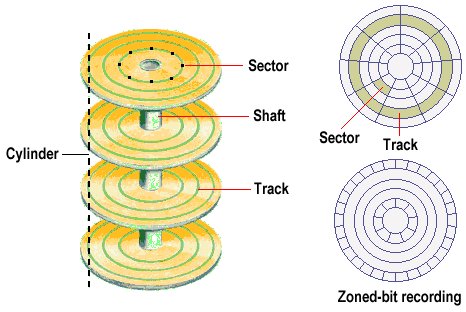
Top View of Disk
- 2 Surfaces per Disk/Platter
- Track – Circular path on a disk surface where data is stored
- Sector – Smallest unit where data can be stored or read
Sector Capacity
Sector Capacity – Constant (Variable Density)
Disk Capacity = 2 × Number of platters × Number of tracks per surface × Number of sectors per track × Sector capacityDisk Access Time
1. Single Sector Access Time
Disk Access Time = Seek Time + Rotational Latency + 1 Sector Transfer Time + Additional Delay2. Multiple Sector Access Time (n sectors sequential in a track)
Disk Access Time = Seek Time + Rotational Latency + ( 1 Sector Transfer Time ) * n + Additional Delay3. Multiple Sector Access Time (n sectors at random location)
Disk Access Time = n * [ Seek Time + Rotational Latency + 1 Sector Transfer Time + Additional Delay ]- Seek Time: Time required to position the arm over the desired track
- Rotational Latency: Time required to rotate the desired sector under the R/W head
- Transfer Time: Time required to read or write 1 sector
where,
Average Rotational Latency = (1 Rotation Time) / 21 Sector Transfer Time = (1 Rotation Time) / (Number of Sectors per Track)Ques.
Seek Time = 10 msSpeed = 6000 RPMSectors per track = 1000Disk Access Time = ? msSolution.
6000 RPM = 6000 rotations per 60 s         = 100 rotations per second
1 Rotation Time = 1 / 100 s                = 0.01 s                = 10 ms
Average Rotational Latency = 10 / 2               = 5 ms
1 Sector Transfer Time = 10 / 1000                       = 0.01 ms
Disk Access Time = Seek + Rotational Latency + 1 Sector Transfer Time                 = 10 + 5 + 0.01                 = 15.01 ms
Disk Transfer Rate
Transfer Rate = Capacity of 1 Track / 1 Rotation Time1 Rotation Time = 1 Track Transfer Time
where,
1 Track Capacity = Number of Sectors per Track × 1 Sector CapacityQues.
1 Rotation Time = 10 msSectors per Track = 1K = 10001 Sector Capacity = 1 KB---Track capacity?Track Rate?Solution:
Track Capacity = 1000 × 1 KB               = 1000 KB               = 10^6 B ≈ 1 MB
Transfer Rate = 1 MB / 10 ms              = (1 MB) / (0.01 s)              = 100 MB/s
DMA with Disk
- All components except CPU & main memory (including cache) are I/O devices.
- Disk is an I/O device.
tx- Disk transfer rate (bytes/sec)ty- CPU I/O service rate (bytes/sec)
% of time CPU blocked = (ty / tx) × 100%Multiple Sectors Access Time
Consider n sequential sectors to be transferred:
= seek time + rotational latency + n * 1 sector transfer time= n * [ seek + rotational latency + 1 sector transfer time]Cylinder
- Cylinder – Collection of all tracks at the same radius (i.e., same track number on every platter).
- Without extra seek time, we can access all sectors on the same cylinder simultaneously (by switching heads).
Disk Addressing in a Cylinder
Addressing Format
< c , h , s > ⬋ ⬇ ⬊ cylinder head sectornt= Number of sectors per tracknc= Number of sectors per cylinder =nt × number of surfaces
Note: It’s for one cylinder only, not the whole disk.
- ✅
nc=nt × number of surfaces - ❌
nc=nt × number of tracks per surface × number of surfaces
Sector Number from Address
Sector No. = (c × nc) + (h × nt) + sAddress from Sector Number
c = floor(sector / nc)h = floor((sector % nc) / nt)s = (sector % nt) % ntPipelining
Section titled “Pipelining”- Pipelining is useful when the same processing is applied to multiple inputs.
- It enables parallel processing by decomposing a sequential process into sub-operations (stages/segments).
- Each stage works on a different task simultaneously.
- First output is obtained after
kcycles (wherek= number of stages). - Thereafter, one output is produced every cycle.
| S1 | S2 | S3 | S4 | |
|---|---|---|---|---|
| 1 | I1 | |||
| 2 | I2 | I1 | ||
| 3 | I3 | I2 | I1 | |
| 4 | I3 | I2 | I1 | |
| 5 | I3 | I2 | ||
| 6 | I3 |
4 Stages → First output after 4th cycles.
Pipeline Cycle Time
- Each stage takes some time.
- The pipeline clock cycle time
tpis chosen as the maximum stage delay.
tp = max(segment delays)Non-Pipelined Execution
- Each task must complete all stages sequentially before the next task starts.
- Time for 1 task:
tn = CPI × 1 Cycle Time- Time for n tasks:
T = n × tnExample (Non-Pipelined)
Cycle |  S1   S2   S3------|---------------   1  | I1   2  |      I1   3  |           I1   ➡ I1 done in 3 cycles   4  | I2   5  |      I2   6  |           I2   ➡ I2 done in 6 cycles   7  | I3   8  |      I3   9  |           I3   ➡ I3 done in 9 cycles
k = 3Total Cycles = n × k = 3 × 3 = 9
Pipelined Execution
- Pipeline with
ksegments - Clock cycle time =
tp ntasks
| Cycles | Time | |
|---|---|---|
| First task | k | k × tp |
Remaining n-1 task | n-1 | (n-1) × tp |
| Total | k+n-1 | (k+n-1) × tp |
Example (Pipelined)
Cycle |  S1   S2   S3------|---------------   1  | I1   2  | I2   I1   3  | I3   I2   I1   ➡ I1 done in 3 cycles   4  |      I3   I2   ➡ I2 done in 4 cycles   5  |           I3   ➡ I3 done in 5 cycles
k = 3Total Cycles = k + (n-1) = 3 + (3-1) = 5
Speed up = (Non Pipelined Time) / (Pipelined Time) = (n * tn) / (k + n - 1)tpSpecial Cases
1. Ideal / Maximum Speedup
- When
n >> k(many tasks relative to pipeline stages):
Max Speedup = tn / tptn= time for 1 task in non-pipelined systemtp= pipeline cycle time
2. Time for 1 task same in pipelined and non-pipelined system
- If
tn = k × tp(task takes exactly k stages × pipeline cycle time):
Max Speedup = kSynchronous Pipeline
Non-Pipeline
- No buffer delay as it is a sequential operation. ⭐
tn = sum of all segment delaysTwo Ways to Find Tn ⭐
Tn = sum of segment delaysTn = CPI * (1 / clock rate)⭐
Pipeline
- Buffer delay occurs due to parallel operations. ⭐
tp = max(segment delays) + register/buffer delay ortp = max(segment delays) (if buffer delay is negligible) Register / Buffer ⬋ ⬋ ⬊ ⬊┌─────┐ ┌─┐ ┌─────┐ ┌─┐ ┌─────┐ ┌─┐ ┌─────┐ ┌─┐│ │ │ │ │ │ │ │ │ │ │ │ │ │ │ ││ S1 │ │ │ │ S2 │ │ │ │ S3 │ │ │ │ S4 │ │ │└─────┘ └─┘ └─────┘ └─┘ └─────┘ └─┘ └─────┘ └─┘Three Ways to Find Tp ⭐
Tp = max(segment delays)(if no buffer/register delay is given)Tp = max(segment delays) + buffer/register delayTp = 1 / clock rate⭐
Latency & Throughput
- Latency - Time taken for a single operation to pass
Latency = k * tp through all k stagesThroughput = (Number of operations) / (Total time taken) = n / [ (k + n - 1) * tp ]Ideal Throughput (when n >> k):
Throughput ≈ 1 / tp- If ideal condition, maximum, or n is not given → assume ideal condition.
Ques. Consider a non-pipelined processor with a clock rate of 100 megahertz and average cycles per instruction of 4. The same processor is upgraded to pipelined processor with 6 stages; but due to the internal pipeline delay, the clock speed is reduced to 75 megahertz. Assume that there are no stalls in the pipeline.
1. The speed up achieved in this pipelined processor for 100 inputs?2. The speed up achieved in this pipelined processor in ideal condition3. If 20% instructions cause 2 stall cycles each, then speed up of pipeline in ideal condition is?Ans.
   Clock_NonPipe = 100x10^(6), CPI = 4   tn = 4 * 1/(100 * 10^(6)) = 4 * 10^(-8)
   Clock_Pipe =  75 x 10^(6) =   tp = 1/ (75 x 10^(6) ) = 10^(-6) / (75)
   n = 100 inputs   k = 6 stages
1.   Clock Speed up = (n * tn) / (k + n - 1)tp                  = [100 * 4 * 10^(-8)] / [(6 + 100 - 1)*10^(-6)/75                  = [4 * 10^(-6)] / [105 * 10^(-6) / 75]                  = [4 * 10^(-6)] * 75 / 105                  =  ~2.86
2.   Ideal clock speed up = tn / tp              = (4 x 10^(-8)) / (10^(-6) / 75)              = (4 x 75) / 100              = 300 / 100              = 3
3. ⭐   Ideal Clock speed up (with Stall) = tn / (CPI * tp)                        = (tn/tp)/CPI                        = 3/CPI                        = 3/1.4  (CPI calculated below)                        = ~2.14
20 % instruction -> 2 stall ⬇                   ⬇Stall freq.         Stall Cycle ⬇                   ⬇0.2                  2
CPI of Pipelined = 1 + (stall freq. * Stall cycles)                 = 1 + 0.2 * 2                 = 1.4
Stall - Extra Cycle due to issue in pipeline For example : Issue like branch instruction - At decode time, cpu don’t know if it take jump or not. till that time cpu do nothing
Stall in Pipelining ⭐
A stall is a delay in the pipeline where a stage must wait before it can proceed, usually because the next stage is not ready or there is a resource/data hazard. It temporarily halts instruction execution in that stage, reducing overall throughput.
Why Stalls Occur:
- Data hazards – An instruction depends on the result of a previous instruction that has not yet completed.
- Control hazards – Branches or jumps whose outcome is not yet known.
- Structural hazards – Two instructions compete for the same hardware resource.
How it Works:
- When a stall occurs, the pipeline inserts bubbles (NOPs) into the stages to delay dependent instructions.
- Other stages may continue executing if they are independent, but the stalled stage waits.
Formula for CPI with Stalls:
CPI_pipeline = CPI_ideal + (Stall frequency * Stall cycles)Where:
CPI_ideal= cycles per instruction without stalls (usually 1 for fully pipelined).Stall frequency= fraction of instructions that cause stalls.Stall cycles= number of cycles the pipeline is stalled per stall-causing instruction.
Effect on Performance:
- Stalls increase Pipeline CPI, decreasing pipeline speedup:
Speedup_with_stall = Tn / (CPI * Tp)- Reducing stalls improves throughput and overall pipeline efficiency.
Instruction Pipeline (with Branch Stall)
5-stage pipeline:
IF - Instruction FetchID - Decode & E.A. CalculationOF - Operand FetchEX - ExecutionWB - Write BackBranch Handling Example:
- Instruction I4 is a branch.
- Until I4’s EX stage completes (Cycle 7), the processor cannot know whether to continue sequentially or jump.
- Because of this uncertainty, the pipeline stalls for 3 cycles (Cycles 5–7).
- Once resolved, the pipeline fetches the correct target instruction (I8) in Cycle 8.
| Instruction | Cycle 1 | Cycle 2 | Cycle 3 | Cycle 4 | Cycle 5 | Cycle 6 | Cycle 7 | Cycle 8 | Cycle 9 | Cycle 10 | Cycle 11 | Cycle 12 | Cycle 13 |
|---|---|---|---|---|---|---|---|---|---|---|---|---|---|
| I1 | IF | ID | OF | EX | WB | ||||||||
| I2 | IF | ID | OF | EX | WB | ||||||||
| I3 | IF | ID | OF | EX | WB | ||||||||
| I4 → Branch | IF | ID | OF | EX | WB | ||||||||
| I5 | Stall | Stall | Stall | ||||||||||
| I6 | Stall | Stall | Stall | ||||||||||
| I7 | Stall | Stall | Stall | ||||||||||
| I8 (Branch Tgt) | IF | ID | OF | EX | WB | ||||||||
| I9 | IF | ID | OF | EX | WB |
Stalls Forumla:⭐
Stalls = Actual cycles − (n + k − 1) orStalls = Target phase − 1 [default: EX = 4 ⇒ 3 stalls]Observations:
n(Instructions executed) = 6 → (I1, I2, I3, I4, I8, I9).k(Pipeline stages) = 5.- Ideal cycles without stall =
n + k - 1 = 6 + 5 - 1 = 10. - Actual cycles with stall = 13.
- Stall cycles inserted = 13 − 10 = 3
or - Stall cycles inserted = target phase − 1 = 4(EX) − 1 = 4-1 = 3
Note: Target phase is the stage where it is decided whether to jump or not.
If target phase is not specified, take Execution (EX) as the default.
Ques. Consider an instruction pipeline with 5 stages without any branch prediction: Fetch Instruction (Fl), Decode Instruction (DI), Fetch Operand (FO), Execute Instruction (El) and Write Operand (WC). The stage delay for Fl, DI, FO, El and WO are 5 ns, 7 ns, 10 ns, 8 ns and 6 ns, respectively. There are intermediate storage buffer after each stage and the delay of each buffer is 1 ns. A program consisting of I2 instructions I1, I2, I3, ......., I12 is executed in this pipelined processor. Instruction I4 is only the branch instruction and its branch target is 19. If the branch is taken during the execution of this program, the time (in ns) needed to complete the program is?
Ans.
Stages (k) : 5 (FI,  DI,  FO,   EI,  WC)Delay    : 5ns, 7ns, 10ns, 8ns, 6nsBuffer Delay = 1nstp = max(5, 7, 10, 8, 6) + 1 = 10 + 1 = 11ns
Branch : I4 -> I9No. of Instructions Stalled : 3 (I5, I6, I7)No. of instructions (n) : 8 (I1, I2, I3, I4,-> I9, I10, I11, I12)Ideal Cycle (without stall) = n + k - 1 = 8 + 5 - 1 = 12Acutal Cycle (with Stall) = 12 + 3 = 15
Time = 14 x 11 = 165 ns
Pipeline Hazard
Situation that prevents the next instruction from executing during its designated clock cycle.
Three Types of Pipeline Hazard
- Structural Hazard / Resource Conflict
- Data Hazard / Data Dependency
- Control Hazard / Branch Difficulty
1. Structural Hazard / Resource Conflict
- Occurs when two different pipeline stages attempt to use the same hardware resource simultaneously.
- Example: ALU required by two instructions. The lower instruction must wait until the upper one completes.
I1 : IF ID OF EX EX WBI2 : IF ID OF - EX WBWhile I1 has not left the execution unit, I2 must wait → 1 Stall
Solution: No practical solution (can be minimized by providing duplicate hardware resources).
2. Data Hazard / Data Dependency
- Occurs when the result of one instruction is required by a subsequent instruction.
- The operand fetch of the second instruction must be delayed until the first instruction’s output is available.
(R1) <------- R2 + R3    ⬊R4 <- R1 * R4
I1 : IF  ID  OF  EX  WBI2 :     IF  ID  -   -   OF  EX  WB
Instruction 2’s Operand Fetch waits for the Write Back of Instruction 1 → 2 Stalls
Solutions:
- Software Solution (by Compiler):
- Delayed Load → Insert a no-operation (NOP) or independent instruction between dependent ones to avoid stall.
- Hardware Solution:
- Operand Forwarding (Bypassing): Eliminates stalls for ALU-to-ALU dependency by forwarding results directly. ⭐
- Hardware Interlock: Detects hazards and introduces necessary stalls automatically.
Note: Not every dependency causes a stall.
Example:
R1 <- R2 + R3R6 <- R5 + R9R8 <- R0 + R4R6 <- R1 * R23. Control Hazard / Branch Difficulty
- Occurs due to branch or jump instructions that change the flow of control, causing incorrect instruction fetch.
Solutions:
- Software Solution (by Compiler): Delayed Branch – rearrange instructions to execute useful work during branch delay.
- Hardware Solution: Branch Prediction – predict the outcome of the branch and continue execution accordingly.
Data Hazard Classification
- Read After Write (RAW) – True Dependency
- Write After Write (WAW) – False Dependency – No Stall
- Write After Read (WAR) – False Dependency – No Stall
1. Read After Write (RAW) – True Dependency
Occurs when an instruction needs to read a value that a previous instruction has not yet written.
I1 : R1 <- R2 + R3I2 : R6 <- R1 * R4I2 cannot read R1 until I1 finishes writing it.
2. Write After Write (WAW) – Write Dependency
Occurs when two instructions write to the same register in sequence.
I1 : R1 <- R2 + R3I2 : R1 <- R4 * R5If both write to R1, the order must be preserved.
-
Solution: Register Renaming
I1 : R1 <- R2 + R3I2 : R8 <- R4 * R5
3. Write After Read (WAR) – Anti-Dependency
Occurs when an instruction writes to a register that a previous instruction still needs to read.
I1 : R1 <- R2 + R3I2 : R2 <- R4 * R5-
Solution: Register Renaming
I1 : R1 <- R2 + R3I2 : R9 <- R4 * R5
Ques. Consider a pipelined processor with the following 4 stages:
IF: Instruction FetchEX: ExecuteID: Instruction Decode and Operand FetchWB: Write BackThe IF, ID, and WB stages take 1 clock cycle each to complete the operation. The number of clock cycles for the EX stage depends on the instruction. The ADD and SUB instructions need 1 clock cycle and the MUL instruction needs 3 clock cycle in the EX stage. Operand forwarding is used in the pipelined processor. What is the number of clock cycles taken to complete the following sequence of instructions?
ADD R2, R1, R0 ; R2 <- R1 + R0MUL R4, R3, R2 ; R4 <- R3 * R2SUB R6, R5, R4 ; R6 <- R5 - R4Ans.
No. of stages (k) = 4No. of instructions (n) = 3
Base cycles (if every EX = 1) = n + k - 1 = 3 + 4 - 1 = 6
EX latencies:- ADD  = 1- MUL  = 3- SUB  = 1
Extra EX cycles relative to 1-cycle EX (per instruction) = (1-1) + (3-1) + (1-1) = 0 + 2 + 0 = 2
Total stalls due to multi-cycle EX (structural) = 2
Total cycles = base cycles + extra = 6 + 2 = 8
Ques. The instruction pipeline of a RISC processor has the following stages: Instruction Fetch (IF), Instruction Decode (ID), Operand Fetch (OF), Perform Operation (PO) and Writeback (WB). The IF, ID, OF and WB stages take 1 clock cycle each for every instruction. Consider a sequence of 100 instructions. In the PO stage, 40 instructions take 3 clock cycles each, 35 instructions take 2 clock cycles each, and the remaining 25 instructions take 1 clock cycle each. Assume that there are no data hazards and no control hazards. The number of clock cycles required for completion of execution of the sequence of instruction is ______ ?
Ans.
k = 5n = 100
Base cycles = n + k - 1 = 100 + 5 - 1 = 104
Extra PO cycles = 40*(3-1) + 35*(2-1) + 25*(1-1)                 = 40*2 + 35*1 + 25*0                 = 80 + 35 + 0                 = 115
Total cycles = 104 + 115 = 219
Pipeline Efficiency
Efficiency = Achieved Speedup / Max SpeedupUsing Times / CPI:
Max Speedup = Tn / TpAchieved Speedup = Tn / (CPI * Tp)=> Efficiency = (Tn / (CPI * Tp)) / (Tn / Tp) = 1 / CPIIf Efficiency is Given (e.g., 80%):
Efficiency = 0.8 = Achieved / Max=> CPI = 1 / Efficiency = 1 / 0.8 = 1.25Interpretation:
- 80% efficiency → Achieved Speedup = 0.8 × Max Speedup
- Efficiency decreases due to stalls (extra cycles increasing CPI)
Ques. Consider a pipeline processor with 4 stages S1 to S4. We want to execute the following loop:
for (i=1; i<=1000; i++) {I1, I2, I3, I4}Where the time taken (in ns) by instruction I1 to I4 for stages S1 to S4 are given below:
S1 S2 S3 S4I1 1 2 1 2I2 2 1 2 1I3 1 1 2 1I4 2 1 2 1The output of I1 for i=2 will be available after
Solution
Loop 1 (i=1) I1 to I4  Time: I1 (1+2+1+2) + I2(2+1+2+1) + I3(1+1+2+1) + I4(2+1+2+1) = 23
Loop 2 (i=2) I1  Time:(1+2+1+2) = 6
Total Time for I2 (i=2) Output = 23+6 = 29
Forumal:
Finish_time(stage j, instr i) = max( Finish_time(stage j, instr i-1), Finish_time(stage j-1, instr i) ) + delay(stage j, instr i)Calculation:
--------- Loop 1 (i=1) ------------
I1-Instruction 1 S1(1) : max(----, ----) + 1 = 0+1 = 1 cycle S2(2) : max(----, S1=1) + 2 = 1+2 = 3 cycle S3(1) : max(----, S2=3) + 1 = 3+1 = 4 cycle S4(2) : max(----, S3=4) + 2 = 4+2 = 6 cycle ⬇ | S1 S2 S3 S4 ---|-------------------➡ I1 | 1 3 4 6 ⬅
I2-Instruction 2 S1(2) : max(I1=1, ----) + 2 = 1+2 = 3 cycle S2(1) : max(I1=3, S1=3) + 1 = 2+1 = 4 cycle S3(2) : max(I1=4, S2=1) + 2 = 4+2 = 6 cycle S4(1) : max(I1=6, S3=6) + 1 = 6+1 = 7 cycle ⬇ | S1 S2 S3 S4 ---|------------------- I1 | 1 3 4 6➡ I2 | 3 4 6 7 ⬅
I3-Instruction 3 S1(1) : max(I2=3, ----) + 1 = 3+1 = 4 cycle S2(1) : max(I2=4, S1=4) + 1 = 4+1 = 5 cycle S3(2) : max(I2=6, S2=5) + 2 = 6+2 = 8 cycle S4(1) : max(I2=7, S3=8) + 1 = 8+1 = 9 cycle ⬇ | S1 S2 S3 S4 ---|------------------- I1 | 1 3 4 6 I2 | 3 4 6 7➡ I3 | 4 5 8 9 ⬅
I4-Instruction 4 S1(2) : max(I3=4, ----) + 2 = 4+2 = 6 cycle S2(1) : max(I3=5, S1=6) + 1 = 6+1 = 7 cycle S3(2) : max(I3=8, S2=7) + 2 = 8+2 = 10 cycle S4(1) : max(I3=9, S3=10) + 1 = 10+1 = 11 cycle ⬇ | S1 S2 S3 S4 ---|------------------- I1 | 1 3 4 6 I2 | 3 4 6 7 I3 | 4 5 8 9➡ I4 | 6 7 10 11 ⬅
--------- Loop 2 (i=2) ------------
I1-Instruction 1 (Loop 2nd) S1(1) : max(I4=6, ----) + 1 = 6+1 = 7 cycle S2(2) : max(I4=7, S1=6) + 2 = 7+2 = 9 cycle S3(1) : max(I4=10, S2=9) + 1 = 10+1 = 11 cycle S4(2) : max(I4=11, S3=11) + 2 = 11+2 = 13 cycle ⬇ | S1 S2 S3 S4 ---|------------------- I1 | 1 3 4 6 I2 | 3 4 6 7 I3 | 4 5 8 9 I4 | 6 7 10 11➡ I1 | 7 9 11 13 ⬅
The output of I1 for i=2 will be available afterAns = 13 nsCPI (Cycles Per Instruction)
With Stalls:
CPI = CPI_ideal + (stall_freq × stall_cycles)For a full pipeline: CPI_ideal = 1=> CPI = 1 + (stall_freq × stall_cycles)Examples:
-
20% instructions → 3 stalls
CPI = 1 + (0.2 × 3) = 1.6 -
20% instructions → 2 stalls
15% instructions → 3 stallsCPI = 1 + (0.2 × 2) + (0.15 × 3) = 1.85 -
10% Branch, 15% ALU, 25% Load, 50% Others
- 5% Branch → 2 stalls
- 50% ALU → 4 stalls
- 1% Load → 20 stalls
CPI = 1 + (0.1×0.05×2) + (0.15×0.5×4) + (0.25×0.01×20) = 1.36
Average Instruction Execution Time
Avg. Execution Time = CPI × TpSpeedup
Speedup = Tn / (CPI × Tp)Efficiency (in terms of stalls)
Efficiency = 1 / [1 + (stall_freq × stall_cycles)]Ques. Consider a 5-stage instruction pipeline, where all stages are perfectly balanced. Assume that there is no cycle-time overhead of pipelining. When an application is executing on this 5-stage pipeline, the speedup achieved with respect to non-pipelined execution if 25% of the instructions incur 2 pipeline stall cycles is ?
Ans.
No. of stages (k) = 5Stages are perfactly balanced -> All Stages Delay time Same
[] [] [] [] []x  x  x  x  x
Speedup- pipelined: tp = max(x,x,x,x,x) = x- non-piplined: tn = x + x + x + x = 5x- 25% instruction -> 2 stall- CPI = 1 + (0.25*2) = 1.5- Speedup = tn /(CPI*tp) = 5x / (1.5 * x) = 3.33
Ans. = 3.33